

A Researcher’s Perspective on Atomic-Scale Imaging
I still remember the first time I saw atomic-scale contrast appear on a Scanning Tunneling Microscope screen. After hours of vibration isolation checks, electronic noise reduction, and tip conditioning, the lattice finally resolved. That moment captures why STM remains essential for serious surface science. For researchers working at the atomic and molecular level, STM is not a luxury – it is a necessity for reliable, high-resolution data.
At Molecular Imaging, STM systems are designed with this research reality in mind. They are built to solve real laboratory challenges such as low noise performance, environmental control, and long-term measurement stability.
What Is the Purpose of STM in Modern Research?
The purpose of STM is to image and analyze conductive and semi-conductive surfaces with atomic and molecular resolution. Unlike optical or electron microscopy, STM directly probes the electronic structure of a surface, making it indispensable in:
- Nanotechnology and surface physics
- Semiconductor research
- Electrochemistry and catalysis
- Molecular electronics
Researchers often ask, “Can STM image molecules?” The answer is yes – when the system offers sufficient mechanical stability, low electronic noise, and precise tip control. Advanced platforms like Molecular Imaging STM systems are engineered to support these requirements across diverse experimental conditions.
What Is the Principle of STM?
Many still ask, “What is the principle of STM?”
STM is based on quantum tunneling. When a sharp conductive tip is brought within a few angstroms of a conductive surface, and a bias voltage is applied, electrons tunnel through the vacuum gap.
The tunneling current:
- Is extremely sensitive to the tip-sample distance
- Changes exponentially with atomic-scale height variations
By maintaining a constant tunneling current while scanning the surface, the STM maps atomic and molecular features with remarkable precision.
This is fundamentally different from questions like “What is STM in ultrasound?” – that refers to Scanning Transmission Methods in acoustics and has no relation to scanning tunneling microscopy used in nanoscience.
Construction of a Scanning Tunneling Microscope
A research-grade STM is not just an instrument; it is a system. The main components include:
- Atomically sharp conductive tip (often tungsten or platinum–iridium)
- Piezoelectric scanners for sub-angstrom positioning
- Vibration isolation and acoustic shielding
- Low-noise electronics and feedback control
- Environmental enclosures (UHV, variable temperature, or electrochemical cells)
Systems such as the Agilent STM and newer Molecular Imaging STM platforms emphasize modular construction, allowing researchers to adapt the microscope to evolving experimental needs rather than replacing entire systems.
Working of STM: From Signal to Data
In operation, the STM tip scans laterally across the surface while maintaining constant tunneling current. The vertical adjustments required to keep this current stable are recorded as topographic data.
Advanced configurations enable:
- Spectroscopy (STS) to probe the local density of states
- Time-resolved measurements
- Bias-dependent imaging
- Molecular manipulation
For experiments requiring real-time environmental control, an In-Situ Scanning Tunneling Microscope allows imaging under electrochemical conditions, variable temperatures, or controlled gas atmospheres – critical for catalysis and battery research.
Applications Across Research Fields
Materials Science & Nanotechnology
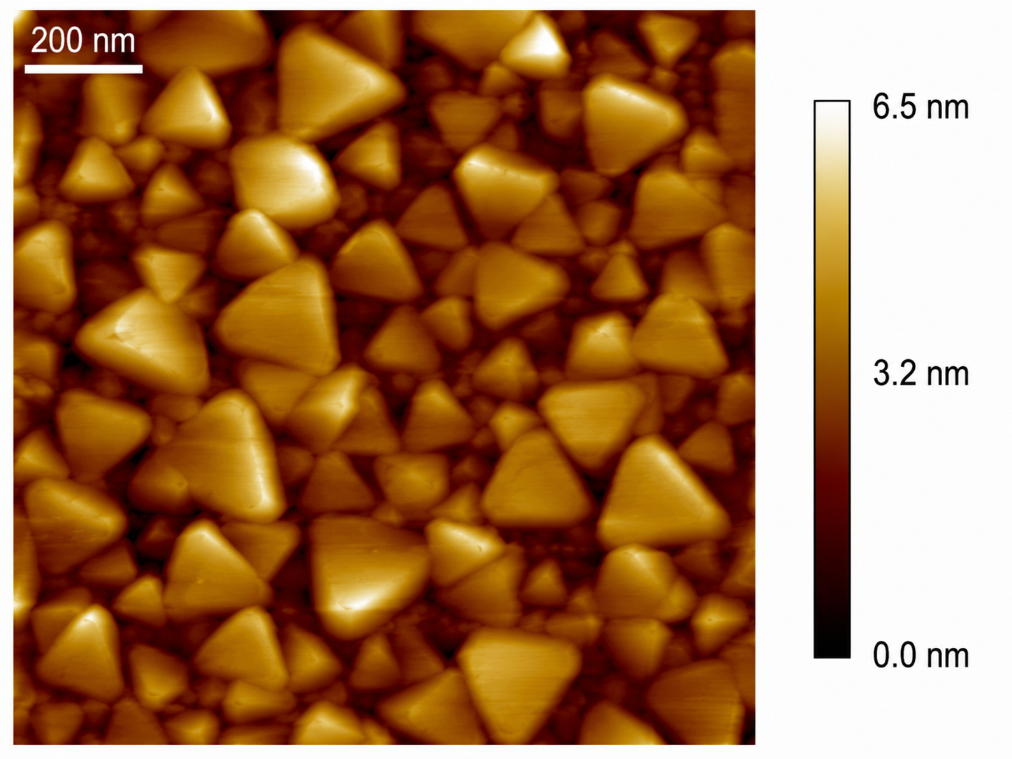
STM enables direct visualization of defects, grain boundaries, and atomic reconstructions that determine material properties at the nanoscale.
Electrochemistry
In-situ STM allows researchers to observe surface reactions during electrochemical processes, bridging the gap between structure and function.
Life Sciences & Molecular Studies
Although STM requires conductive samples, molecular imaging on functionalized substrates has expanded its relevance in biological and chemical research.
Reliability, Service, and Long-Term Research Value
High-resolution data depends not only on design but also on long-term performance. Access to professional STM service and STM repair is essential to maintain accuracy, reduce downtime, and extend instrument lifespan.
Molecular Imaging focuses on:
- Serviceable, upgrade-ready systems
- Long-term mechanical and electronic stability
- Research continuity over years – not product cycles
Why Modular STM Systems Matter
Modern research evolves quickly. Modular STM platforms allow laboratories to:
- Add new measurement modes
- Upgrade electronics without replacing mechanics
- Adapt systems for new materials or environments
This flexibility directly improves research efficiency, reproducibility, and funding return on investment.
Conclusion: STM as a Research Partner, Not Just an Instrument
So, what is the purpose of STM today? It is not simply imaging – it is understanding matter at its most fundamental level. With atomic precision, controlled environments, and dependable performance, STM remains a cornerstone of surface science.
By combining deep technical expertise, modular design philosophy, and long-term support, Molecular Imaging positions itself as a trusted technology partner for researchers who demand accuracy, stability, and scientific credibility – today and for the next generation of discovery.
Post a comment
Related Posts
May 15, 2026
Why High Quality AFM Data Matters for Your Research
Modern research environments demand more than visually impressive nanoscale images. Researchers working in nanotechnology, semiconductor…