

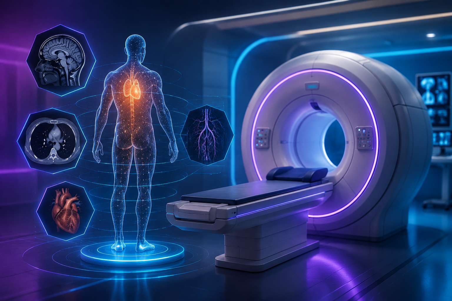
Scientific research at the nanoscale depends heavily on imaging accuracy, environmental stability, and reproducible data. Whether researchers are analyzing biomolecular interactions, thin films, nanomaterials, or semiconductor surfaces, the ability to capture highly detailed structural information directly influences the quality of experimental outcomes. Traditional imaging techniques often struggle to provide the resolution, flexibility, and quantitative analysis required in modern research laboratories.
This is where Advanced Imaging Solutions play a critical role. Modern imaging technologies combine high-resolution hardware, precision environmental controls, intelligent data processing, and modular system architecture to help researchers study materials and biological structures at the atomic and molecular scale.
At Molecular Imaging, these advanced solutions are designed specifically for research environments that demand low noise, experimental flexibility, and long-term data reliability.
Understanding Advanced Imaging Solutions in Scientific Research
Advanced imaging systems are specialized analytical technologies that allow researchers to visualize, measure, and analyze nanoscale structures with exceptional precision. These Advanced Imaging Solutions support applications across materials science, biotechnology, nanotechnology, and semiconductor research.
In scientific instrumentation, advanced imaging is not limited to simply producing clearer images. These systems are built to support highly controlled experiments involving molecular interactions, surface mechanics, electrochemical reactions, and biological processes. Researchers depend on stable imaging conditions to minimize artifacts, reduce thermal drift, and improve quantitative consistency across datasets.
Modern imaging platforms integrate several critical technologies to improve performance:
- High-resolution scanners for nanoscale accuracy
- Low-noise electronics for stable signal acquisition
- Environmental isolation systems to reduce vibration and contamination
- Automated processing software for artifact correction and data optimization
- Modular architecture for experimental flexibility
For laboratories conducting highly specialized studies, imaging precision directly affects publication quality, reproducibility, and scientific credibility.
How Does Advanced AFM Imaging Work?
High-Resolution Surface Characterization
One of the most widely used imaging methods in nanoscale research is AFM (Atomic Force Microscopy). AFM works by scanning a highly sensitive probe across the sample surface to generate detailed three-dimensional topographical maps at nanometer or even atomic-scale resolution.
Unlike optical microscopy, which is limited by the wavelength of light, AFM relies on tip-sample interactions to detect extremely small surface variations. As the cantilever probe moves across the sample, tiny deflections are measured using laser detection systems and converted into highly detailed surface data.
This approach allows researchers to study:
- Surface roughness and morphology
- Nanoparticle distribution
- Thin-film uniformity
- Mechanical properties such as stiffness and adhesion
- Molecular and biomaterial structures
AFM is especially valuable because it can analyze delicate biological samples and soft materials without requiring destructive preparation methods. Researchers can image proteins, DNA, lipid membranes, and living cells in liquid environments while preserving their native structure.
Environmental Stability and Controlled Imaging Conditions
High-resolution imaging depends heavily on environmental control. Even small fluctuations in temperature, humidity, or vibration can distort nanoscale measurements and reduce data accuracy. This is particularly challenging during long-duration experiments or force spectroscopy applications where thermal drift may compromise reproducibility.
To overcome these issues, advanced AFM systems often integrate a dedicated Environmental Chamber that isolates the imaging process from external disturbances. These chambers help reduce acoustic interference, airborne contamination, and environmental instability while maintaining consistent imaging conditions throughout the experiment.
Researchers working with temperature-sensitive materials or electrochemical systems may also require a Temperature Controlled Chamber to maintain stable thermal conditions during imaging. Controlled temperature environments are essential for studies involving polymers, biomaterials, phase transitions, and nanoscale chemical reactions where thermal fluctuations can influence material behavior.
Stable environmental control significantly improves signal clarity, reduces imaging artifacts, and supports more reproducible datasets across multiple experiments.
Applications of Advanced Imaging Across Research Fields
Life Sciences and Biotechnology
Biological research often involves highly sensitive samples that require non-destructive imaging techniques. Advanced AFM systems allow researchers to study cellular structures, biomolecular assemblies, and tissue mechanics under near-physiological conditions.
In biotechnology and medical research, scientists frequently investigate nanoscale interactions between proteins, membranes, and living cells. High-quality imaging supports force spectroscopy measurements used to analyze molecular adhesion, receptor binding, and cellular elasticity. These capabilities are increasingly important in cancer research, drug development, and tissue engineering applications.
The ability to combine fluid imaging, nanomechanical mapping, and environmental control within a single platform makes AFM highly valuable for interdisciplinary life science research.
Materials Science and Semiconductor Research
Advanced imaging also plays a central role in materials characterization and semiconductor development. Researchers use AFM to evaluate thin films, nanocomposites, coatings, graphene structures, and semiconductor surfaces with extremely high precision.
Detailed nanoscale analysis helps scientists understand how surface morphology and mechanical behavior affect conductivity, durability, and device performance. In semiconductor manufacturing, even minor nanoscale defects can influence fabrication yield and operational reliability.
Modern modular imaging platforms allow researchers to integrate multiple experimental modes for electrical measurements, electrochemical analysis, and nanomechanical testing within one system. This flexibility improves laboratory efficiency while supporting more advanced scientific workflows.
Why Modular Imaging Platforms Improve Research Efficiency
Research laboratories rarely operate under fixed experimental conditions. As projects evolve, scientists often require additional imaging modes, environmental controls, or analytical capabilities to support new applications. Modular AFM systems provide long-term flexibility by allowing researchers to customize their imaging setup without replacing the entire platform.
At Molecular Imaging AFM solutions, modular system architecture helps laboratories adapt to changing research requirements while maintaining imaging performance and data consistency. Researchers can integrate fluid imaging, spectroscopy tools, advanced force measurements, and environmental controls depending on their application needs.
This flexibility is particularly valuable for multidisciplinary research groups working across nanotechnology, electrochemistry, biotechnology, and semiconductor science. Scalable imaging platforms improve operational efficiency while supporting future research expansion.
Although some institutions initially compare systems based on Atomic Force Microscope Price, long-term scientific value depends more heavily on data quality, system stability, technical support, and experimental adaptability. Reliable imaging platforms help reduce downtime, improve reproducibility, and support publication-quality research over many years of operation.
Ready to Improve Your Research Imaging Capabilities?
Explore customizable AFM platforms, environmental imaging systems, and advanced nanoscale characterization technologies from Molecular Imaging. Whether your laboratory focuses on biotechnology, materials science, nanotechnology, or semiconductor research, the right imaging solution can help strengthen data accuracy, reproducibility, and long-term research performance.
Conclusion
Advanced imaging technologies have become essential tools for researchers working at the nanoscale. High-resolution imaging, environmental stability, and modular flexibility allow scientists to generate more accurate and reproducible datasets across life sciences, materials science, electrochemistry, and semiconductor research.
Modern AFM systems provide far more than visual surface analysis. They support quantitative nanoscale characterization, nanomechanical mapping, molecular interaction studies, and highly controlled experimental workflows that strengthen long-term scientific outcomes.
By combining customizable instrumentation with application-focused expertise, Molecular Imaging helps research laboratories improve imaging precision, workflow efficiency, and data reliability for advanced scientific discovery.
FAQs
What resolution can Atomic Force Microscopy achieve?
Atomic Force Microscopy can achieve vertical resolution below 0.1 nanometers and lateral resolution typically ranging from 1 to 50 nanometers, depending on the probe tip and sample properties.
What factors affect Atomic Force Microscopy resolution?
AFM resolution is affected by probe tip sharpness, scan speed, environmental vibrations, thermal drift, sample roughness, and imaging mode.
Is Atomic Force Microscopy higher resolution than optical microscopy?
Yes. AFM provides nanoscale surface measurements that are significantly higher in resolution than conventional optical microscopy.
How does Atomic Force Microscopy achieve high resolution?
AFM uses a sharp probe tip that scans the sample surface and measures nanoscale height variations through tip-sample interactions, enabling extremely detailed surface characterization.
What is the difference between lateral and vertical resolution in AFM?
Vertical resolution measures the smallest detectable height change, while lateral resolution measures the smallest detectable feature size across the sample surface.
Can AFM image individual molecules?
Yes. Under optimized conditions, high-resolution atomic force microscopy can image individual molecules, proteins, DNA structures, and atomic-scale surface features.
What industries rely on high-resolution Atomic Force Microscopy?
High-resolution AFM is widely used in semiconductor research, nanotechnology, materials science, biotechnology, electrochemistry, and biomedical engineering.