


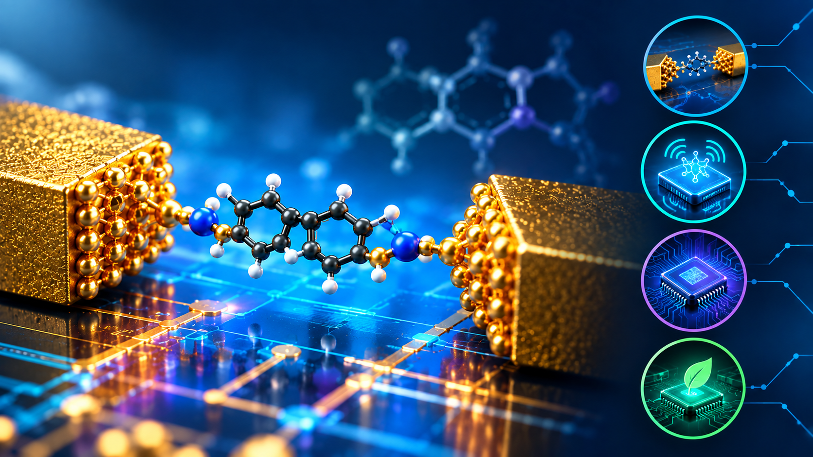
When electronic behavior depends on what’s happening at the molecular scale, conventional electrical measurements only tell part of the story; they can’t show how individual molecules are arranged, how they contact an electrode, or where conduction changes across a surface.
This is why molecular electronics applications are studied using scanning probe techniques such as atomic force microscopy (AFM) and scanning tunneling microscopy (STM), which connect molecular structure directly to nanoscale electrical behavior. STM measures tunneling current to probe electronic states with atomic resolution, while conductive AFM and related electrical AFM modes combine surface imaging with current, voltage, and potential measurements.
Together, these techniques let researchers investigate molecular junctions, self-assembled molecular layers, and other structures central to organic molecular electronics and nano-electronics research.
What is Molecular Electronics?
Molecular electronics is the study of electronic functions in which individual molecules or molecular assemblies play an active or passive role in charge transport, switching, sensing, or related device behavior. Research commonly examines how molecular structure, electrode interfaces, molecular orientation, and contact geometry influence electron transport.
This makes nanoscale characterization particularly important. A molecular device cannot be understood from electrical measurements alone because the measured response also depends on the molecule-electrode interface and the physical structure of the junction.
How Does STM Support Molecular Electronics Research?
STM is especially useful when researchers need to study conductive surfaces and molecular-scale electronic behavior. The technique uses a conductive tip positioned extremely close to a conductive sample. A tunneling current flows across the gap, allowing the system to generate topographic information and, with appropriate measurement modes, investigate local electronic properties.
For molecular electronics, STM can be used to:
- Examine molecules and molecular assemblies on conductive substrates
- Study molecular-scale surface structure
- Measure local tunneling current
- Investigate electronic states using scanning tunneling spectroscopy
- Form or investigate nanoscale molecular junctions
- Explore relationships between molecular structure and conductance
STM-based approaches are particularly important for single-molecule electronics because an STM tip can serve as one electrode while the substrate provides another, creating a controllable nanoscale junction. STM break-junction methods are also established approaches for measuring charge transport through individual molecules.
How Does AFM Contribute To Molecular Electronics Applications?
AFM can image electrically insulating as well as conductive samples, making it useful for characterizing molecular layers, polymers, nanostructures, and interfaces that may not be suitable for conventional STM.
For molecular electronics, specialized AFM modes become particularly relevant.
Conductive AFM
Conductive AFM, or C-AFM, combines surface imaging with local current measurements. A conductive probe contacts or interacts with the sample while an electrical bias is applied, allowing researchers to map variations in conductivity across a surface.
This can help investigate:
- Conductive and insulating regions
- Molecular films
- Nanostructured conductive materials
- Electrical behavior across interfaces
- Local variations in current flow
Kelvin Force and Related Electrical Measurements
Kelvin Force Microscopy (KFM) and Electrostatic Force Microscopy (EFM) map contact potential difference and surface charge without requiring direct electrical contact.
For organic molecular electronics, this is particularly valuable: KFM can resolve surface potential contrast from molecular dipoles, distinguish doped regions in organic semiconductors, and image charge distribution across self-assembled molecular structures, information that complements the current maps produced by C-AFM.
The Molecular Imaging image gallery includes Kelvin force microscopy examples involving an IC chip, carbon nanotubes, and graphene bridged between electrodes.
How are Molecular Junctions Characterized?
A molecular junction typically places a molecule, or molecular assembly, between two electrodes so researchers can examine charge transport through the molecular system.
The challenge is that the electrical signal depends on more than the molecule itself. Electrode material, contact geometry, anchoring groups, molecular orientation, and the surrounding environment can all influence the measured conductance.
STM and AFM-based approaches can therefore be used as part of a broader characterization workflow:
- Characterize the substrate to establish surface condition and structure.
- Image molecular assemblies to understand their distribution and morphology.
- Establish electrical contacts using an appropriate probe or junction method.
- Measure current or conductance under controlled conditions.
- Compare electrical behavior with structural information to understand the molecule-electrode relationship.
This combination is important because a conductance measurement without structural context can be difficult to interpret reliably.
What Role Do AFM And STM Play in Organic Molecular Electronics?
Organic molecular electronics focuses on electronic behavior involving organic molecules, molecular films, and related carbon-based materials. AFM can help characterize morphology, roughness, mechanical behavior, and local electrical properties, while STM can provide atomic- or molecular-scale information on conductive surfaces and tunneling behavior.
For example, self-assembled monolayers can be examined to understand how molecules organize on a conductive substrate before electrical characterization. STM-based methods can then investigate local electronic behavior, while conductive AFM can provide spatially resolved electrical information over suitable samples. Research literature identifies both STM and conducting-probe AFM as important scanning-probe approaches for molecular electronic systems.
Can These Techniques Be Used For Electrochemical Molecular Electronics?
Yes. Molecular electronics research can also involve electrochemical environments where molecular charge transport is affected by electrode potential, redox processes, or the surrounding electrolyte.
STM and AFM systems configured for electrochemical work can support measurements under controlled liquid conditions. Molecular Imaging published materials include electrochemical AFM/SPM capabilities, electrochemical accessories, liquid-cell components, and examples of in-situ electrochemical imaging.
Researchers can therefore combine structural imaging with electrical or electrochemical measurements when studying interfaces, molecular assemblies, electrode surfaces, and related nanoscale processes.
How Should Researchers Choose Between AFM And STM?
The appropriate technique depends on the material, measurement objective, and electrical configuration.
| Research objective | Useful technique |
| Surface topography of nonconductive materials | AFM |
| Local conductivity mapping | Conductive AFM |
| Surface potential measurements | Electrical AFM methods such as KFM |
| Atomic-scale imaging of conductive surfaces | STM |
| Local tunneling current | STM |
| Single-molecule junction studies | STM and break-junction approaches |
| Molecular layers and surface morphology | AFM or STM, depending on sample |
| Electrochemical interface studies | Electrochemical AFM/STM configurations |
Molecular Imaging’s application and publication resources can also help researchers explore AFM and STM approaches used across molecular electronics and related nanoscale research.
Conclusion
AFM and STM provide complementary ways to investigate molecular electronics applications, from molecular-layer morphology and local conductivity to tunneling current and single-molecule charge transport. The most useful technique depends on the sample and the research question, but combining structural and electrical characterization can provide a more complete picture of nanoscale electronic behavior.
For researchers working with molecular junctions, conductive materials, or molecular assemblies, choosing the right AFM or STM configuration starts with understanding what needs to be measured. Explore Molecular Imaging’s AFM and STM systems and application resources to see which approach best fits your research.
FAQs
What is the main use of STM in molecular electronics?
STM is commonly used to investigate conductive surfaces, molecular assemblies, tunneling current, and local electronic properties. STM-based junction techniques can also measure charge transport through individual molecules.
What are molecular electronics devices?
Molecular electronics devices use individual molecules or molecular assemblies as functional elements for electronic behavior such as switching, sensing, rectification, or charge transport.
What’s the difference between AFM and STM for molecular electronics?
AFM characterizes molecular structure, surface morphology, and local electrical properties, while STM measures tunneling current and electronic behavior on conductive surfaces. Both can help researchers study molecular assemblies and molecular junctions, but they use different probe-sample interactions.
How is AFM used to study molecular electronics?
AFM helps researchers examine molecular layers, surface morphology, and local conductivity at the nanoscale. Conductive AFM can also map current variations across suitable molecular and conductive materials.
How is STM used to study molecular electronics?
STM images molecules and conductive surfaces while measuring tunneling current and local electronic properties. It can also be used to investigate molecular junctions and charge transport through individual molecules.