Introduction
Nanoparticle research keeps growing more demanding. Whether you're developing drug-delivery systems, engineering battery materials, or studying nanocomposite coatings, one question keeps surfacing: how do you actually measure something 100,000 times thinner than a human hair with confidence?
Many researchers struggle with this exact problem:
- Optical microscopes can't resolve features below roughly 200 nanometers
- Bulk techniques like DLS report averages, not individual particle shapes
- Electron microscopy delivers stunning detail but flattens everything into a 2D projection, and requires vacuum plus heavy sample prep that can distort delicate biological or organic nanoparticles
Atomic Force Microscopy (AFM) fills this gap. It generates true three-dimensional surface data, works in air, vacuum, or liquid, and handles everything from rigid metal nanoparticles to fragile liposomes.
Below you’ll find how AFM works, a practical characterization workflow, the nanoparticle properties it can quantify, and guidance on choosing the right system for your lab.
Key Takeaways
- AFM produces genuine 3D height data, unlike the 2D projections from SEM/TEM
- Height accuracy reaches sub-nanometer levels, even when lateral resolution is limited by tip geometry
- Reliable size distributions typically require imaging at least 100 isolated particles
- Works in air, vacuum, and liquid—suitable for both biological and inorganic samples
- Sample prep and tip selection directly determine measurement accuracy
What Is Atomic Force Microscopy (AFM)?
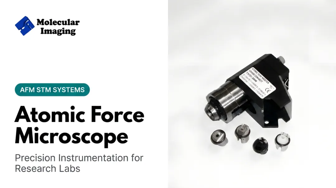
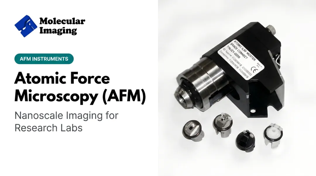
Atomic force microscopy (AFM) is a form of scanning probe microscopy (SPM). Rather than bouncing light or electrons off a sample, it physically "feels" the surface with a sharp cantilever tip, translating the tip's movement into an image.
Here's the core mechanism: a laser reflects off the back of the cantilever onto a photodiode. As the tip traces the sample surface, cantilever deflection changes the laser's position on the detector. That signal gets converted into a topographic height map, point by point, as described in the NIST-hosted AFM nanoparticle sizing protocol.
The result is a true three-dimensional surface profile, often called a 2.5D reconstruction because it captures height at every X-Y coordinate. SEM and TEM produce 2D projections. That difference is critical for nanoparticle sizing, where height data is far less distorted by probe geometry than lateral width measurements.
AFM also operates in air, vacuum, or liquid. That flexibility makes it equally suited to inorganic nanoparticles dried on a wafer and biological nanostructures suspended in their native aqueous environment.
Imaging Modes Used for Nanoparticles
Selecting the right mode matters as much as selecting the right tip. Three modes dominate nanoparticle work:
- Contact mode — Tip stays in direct contact. Strong for rigid, well-adhered particles; can drag or damage soft or loosely bound samples.
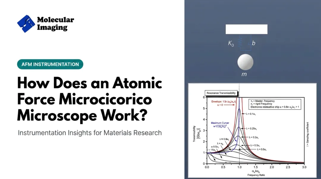
- Intermittent contact (tapping) mode — Cantilever oscillates near resonance and taps briefly, cutting lateral forces. Preferred for most nanoparticle height work.
- Non-contact mode — Tip senses long-range forces without touching. Best for very soft or fragile nanostructures.
For most nanoparticle sizing work, tapping mode strikes the best balance between resolution and sample preservation.

How AFM Characterizes Nanoparticles: The Step-by-Step Process
Turning a nanoparticle sample into reliable size and shape data follows a defined workflow. Skip a step, and your measurements suffer.
Sample Preparation
Nanoparticles need to sit isolated on an ultra-flat substrate so the AFM can measure them individually rather than as a jumbled mass. Common substrates include:
- Mica — cleaves to reveal an atomically flat surface
- Single-crystal silicon — stable and widely available
- Gold (Au) — useful for thiol-based functionalization Substrate roughness must stay far smaller than the particles themselves, so researchers often functionalize the surface to hold particles in place. Poly-L-lysine (typically 0.1%) gives mica a positive charge that attracts negatively charged citrate-stabilized gold nanoparticles. Silane coupling agents serve a similar role on silicon. Without this step, particles can shift or aggregate during scanning and ruin the dataset.
Imaging and Scanning Parameters
With particles fixed on the substrate, tip selection and scan setup drive measurement accuracy. Tips with a radius below roughly 10 nanometers reduce the "tip convolution" effect that inflates lateral measurements. Cantilever stiffness matters too. It should roughly match or sit slightly below the sample's own stiffness so the probe deforms the particle as little as possible. Before collecting real data, calibrate the instrument's z-piezo against a traceable height standard. One documented protocol used a certified 19.5 ± 0.8 nm SiO2 step-height grating, chosen specifically because its height resembled the nanoparticles under study. Matching your calibration standard height to your expected particle size is what makes your height data defensible.
Data Analysis and Size Determination
Raw AFM images almost always show a slight tilt from imperfect sample mounting. Flattening or leveling the image removes this artifact before any measurement happens. Once leveled, researchers extract a cross-sectional profile through the center of each particle. The top-height value from that profile becomes the standard measurement for calculating diameter, for spherical or rod-shaped particles alike—height is far less affected by tip geometry than lateral width. How many particles is enough? A 2022 metrological study on AFM tip characterization found that imaging around 100 particles produces statistically sound results, reporting datasets ranging from 100 to 120 particles depending on sample type. Fewer than that, and your size distribution risks skewing toward whatever particles happened to land in your scan area.

Key Nanoparticle Properties You Can Measure With AFM
Height and diameter are just the starting point. A well-configured AFM setup can pull multiple property classes from the same sample in one session.
Height and diameter. Isolated-particle top-height measurements routinely achieve sub-nanometer accuracy, whether particles are spherical, rod-shaped, or irregularly faceted.
Lateral dimensions and morphology. Shape, faceting, and aspect ratio can all be reconstructed from AFM scans. One caveat: tip geometry affects lateral resolution far more than it affects height accuracy, so shape data should always be interpreted alongside known tip dimensions.
Mechanical properties. Force-distance spectroscopy modes map:
- Stiffness and elastic modulus
- Adhesion forces between tip and particle
- Deformation and viscoelastic behavior
- Energy dissipation during contact
Surface roughness. Topographical mapping reveals roughness parameters relevant to coatings, thin films, and nanocomposites, useful well beyond individual particle sizing.
Combined electrical/chemical mapping. Hyphenated techniques like Kelvin Probe Force Microscopy (KPFM) capture surface potential and work function alongside topography in a single pass.
One 2025 study using KPFM on TiO2 nanoparticles sized 3–85 nm reported work function values between 4.49 and 4.57 eV — electrical and structural data from the same scan, not separate instruments.
Advantages of AFM Over Other Nanoparticle Characterization Techniques
Every characterization method has tradeoffs. Here's how AFM stacks up:
| Technique | Dimensionality | Sample Environment | Key Limitation |
|---|---|---|---|
| AFM | True 3D topography | Air, vacuum, or liquid | Lateral resolution tied to tip geometry |
| SEM/TEM | 2D projection | Requires vacuum | Extensive prep, potential coating artifacts |
| DLS | Hydrodynamic size only | Solution-based | Struggles with polydisperse samples |
DLS measures a hydrodynamic diameter that includes solvent and ionic layers around the particle, not the particle itself. TEM often captures just the metallic core. AFM measures the deposited particle as it actually sits, giving a distinct but equally valid measurand.
AFM also handles sample types other techniques struggle with. It images conductive, insulating, organic, and biological nanoparticles without conductive coatings. Samples can be characterized directly in liquid, which helps preserve native conformation for biological nanostructures.
No method is perfectly accurate. A 2024 VAMAS interlaboratory comparison spanning 21 laboratories using TEM, SEM, and AFM found size deviations of roughly 10% across techniques, with AFM showing a slight negative bias and SEM a slight positive one.
No single method wins outright. AFM's edge is height fidelity and native-environment imaging, not universal superiority.
Common Challenges and Limitations in AFM Nanoparticle Analysis
AFM nanoparticle analysis has a few recurring limitations. Three come up most often:
- Tip dilation (convolution) effects. A finite tip radius makes lateral measurements appear larger than the actual particle, especially when particles sit close together or have complex shapes. This is why height, not width, is the preferred sizing metric.
- Sample preparation artifacts. Incomplete dispersion or drying-induced aggregation can clump particles so software reads several as one feature—or splits one into many. VAMAS work flagged agglomeration as a driver of false segmentation that skews size and count.
- Throughput limitations. Unlike bulk techniques that process thousands of particles in seconds, AFM requires scanning isolated particles individually. Reaching the recommended 100+ particle threshold for statistically sound distributions takes real time, though far less than manually curating equivalent TEM datasets.
None of these rule AFM out. They do mean nanoparticle work rewards careful protocol design over rushed scanning sessions.
Choosing the Right AFM System for Your Nanoparticle Research
Picking an AFM platform for nanoparticle work comes down to three practical questions: can it switch imaging modes without a full teardown, can it control the sample environment, and does the software actually support quantitative analysis?
Modularity matters because nanoparticle projects rarely stay in one lane. A researcher might start with tapping mode for basic sizing, then need force spectroscopy for mechanical mapping, then KPFM for surface potential, all on the same sample set.
Environmental control is equally non-negotiable. Temperature-dependent phase transitions, humidity-sensitive aggregation, and liquid-phase biological imaging all demand hardware built for those conditions—not bolted on afterward.
Quantitative analysis closes the loop. Sizing alone is rarely enough; force curves, surface potential maps, and mechanical property data need modes and software that export reproducible numbers, not just images.
Molecular Imaging's 5500 PicoPlus AFM+STM and 5500 ILM PicoPlus BioAFM platforms address these needs directly:
- Modular nose cone design for fast switching between AFM, STM, tapping mode, KPFM, MFM, and force spectroscopy without swapping the scanner
- Temperature-controlled stages from -30°C to 250°C for thermal stability and phase-transition studies
- Environmental Isolation Chambers for humidity, low-oxygen, and reactive gas conditions
For labs already running legacy Agilent-era AFM/STM systems, a full replacement isn't always required. Molecular Imaging's ZoomAFM repair and calibration service covers diagnostics, hardware repair, and precision recalibration with platform-matched parts—extending the working life of instruments already suited to nanoparticle work.

Frequently Asked Questions
Is AFM a microscopy technique?
Yes. AFM is a form of scanning probe microscopy that generates images by physically scanning a sharp tip across a sample surface, rather than using light or electron beams like optical or electron microscopy.
How can AFM be used to characterize nanoparticles?
AFM measures nanoparticle height, diameter, shape, and surface properties by scanning isolated particles deposited on flat substrates like mica or silicon, then extracting cross-sectional height profiles for size calculation.
What size range of nanoparticles can AFM accurately measure?
AFM resolves particles from a few nanometers up to several hundred nanometers, with height accuracy typically reaching the sub-nanometer level, though lateral resolution depends on tip geometry.
Can AFM be used to image nanoparticles in liquid or biological environments?
Yes. Specialized BioAFM systems and liquid cells allow imaging of nanoparticles, proteins, and cells in near-native aqueous conditions, often using MAC Mode to avoid acoustic noise artifacts common in standard liquid tapping.
How does AFM compare to SEM or TEM for nanoparticle sizing?
AFM offers true 3D height data without vacuum requirements, while SEM and TEM provide higher lateral resolution but only 2D projections. Each method measures a slightly different aspect of particle size.
Does AFM require special sample preparation for nanoparticles?
Yes. Nanoparticles must be dispersed on an atomically flat, often functionalized substrate, such as poly-L-lysine-treated mica, to ensure isolated, stable imaging and accurate height measurements.