Atomic force microscopy sits at an unusual intersection here. The same instrument that images a surface at sub-nanometer resolution can also pattern that surface directly, with no photomask or vacuum chamber required.
This guide walks through how AFM lithography works, the characterization modes researchers pair with it, where the technique shows up across industry, and how to pick a system that does both jobs well.
Key Takeaways
- AFM lithography creates sub-100nm patterns without the cleanroom infrastructure that e-beam or photolithography demands
- Bias-assisted oxidation and force-assisted scratching are the two dominant lithography mechanisms
- Characterization modes like C-AFM, KPFM, and PeakForce QNM map electrical and mechanical properties at the nanoscale
- Modular AFM/STM platforms let one instrument handle both patterning and imaging in a single workflow
Understanding AFM Fundamentals
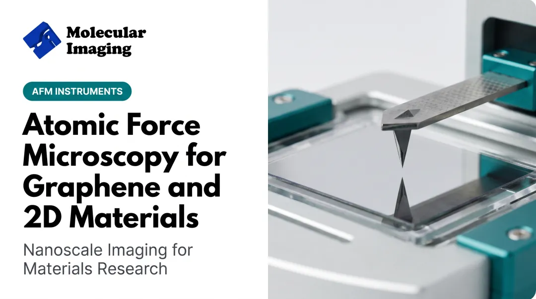
An AFM uses a few core components: a sharp tip mounted on a flexible cantilever, a laser bounced off that cantilever onto a photodetector, and a feedback loop that controls tip-sample force. The original 1986 AFM paper described the concept as combining scanning tunneling microscopy principles with a stylus profilometer, using a probe gentle enough not to damage the surface it's measuring.
As the tip scans, the feedback loop maintains constant force or oscillation amplitude, translating tiny cantilever deflections into a topographic map.
Three Core Imaging Modes
- Contact mode — tip stays in continuous contact with the surface; good for hard samples, less suited to soft biological material
- Tapping mode — cantilever oscillates near resonance, touching down intermittently; reduces damage to delicate samples
- Non-contact mode — tip hovers above the surface, sensing attractive forces; gentlest option, best for fragile or contamination-sensitive samples
AFM also stands out for environmental range. It runs in air, liquid, and vacuum, which is why it shows up in semiconductor fabs, materials labs, and life science facilities alike. Liquid-based BioAFM can image single molecules, bacteria, and living cells directly in buffer.

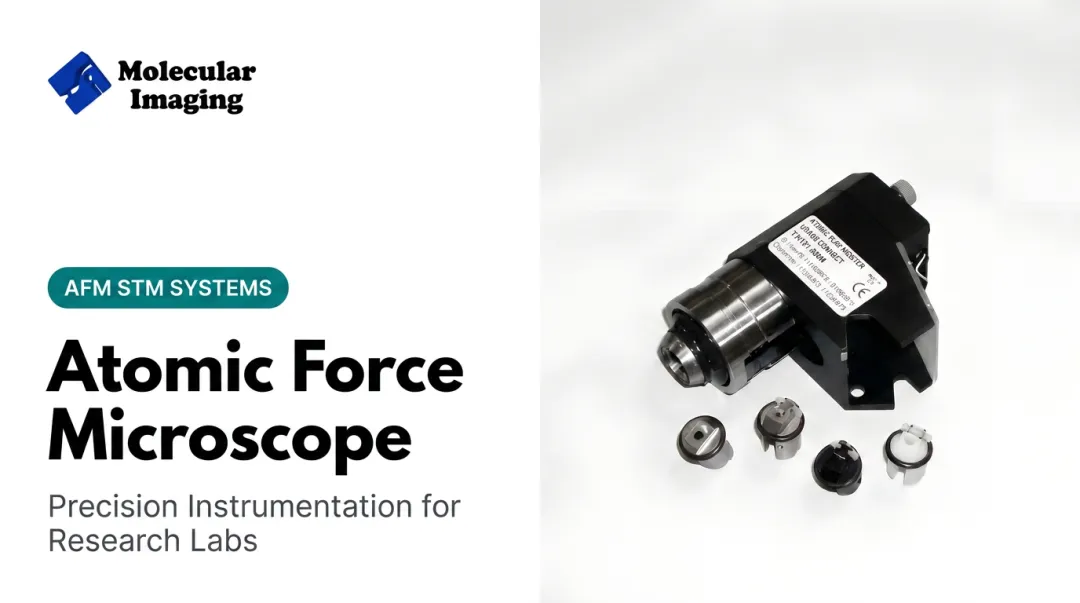
Molecular Imaging's 5500 PicoPlus and 5420 PicoAFM platforms reflect this range, with liquid-cell designs compatible with acidic, basic, and organic-solvent media alongside standard ambient-air operation.
AFM Nanolithography Techniques
AFM nanolithography lets researchers pattern surfaces at the nanoscale without electron-beam or focused-ion-beam infrastructure. A 2022 scanning-probe-lithography review notes that EBL and FIB carry higher startup costs and vacuum requirements, while scanning-probe methods offer lower equipment complexity for prototype-scale work, though throughput can run slower than EBL in some configurations.
Two mechanisms dominate:
Bias-Assisted Local Anodic Oxidation
A voltage applied between tip and sample generates a local electric field strong enough to oxidize the substrate underneath. A 2002 study on silicon surfaces produced oxide lines with a 7nm top width, 20nm base width, and 13nm periodicity, reaching sub-20nm patterning.
Local anodic oxidation also works on metal films. A 1998 study oxidized titanium up to 8nm thick on GaAs, though the resulting oxide spots ran several hundred nanometers in diameter, a very different geometry than the silicon linewidth example.
Force-Assisted Mechanical Scratching
Here, the tip simply pushes harder. Increased contact force displaces surface material mechanically, carving grooves into polymer-like samples. One documented experiment produced a polycarbonate grating measuring 100 µm × 150 µm with a 500nm period and 50nm groove depth. A 2022 review also cites a sub-20nm line with roughly 1nm depth cut into GaAs.

Molecular Imaging's lithography demonstrations on the Agilent 5500 platform include:
- Repeating line patterns on polymer
- Nested squares on Au(111)
- Dot arrays on polycarbonate
One example, an AFM-written signature on polycarbonate, shows measured vertical features between 17.5nm and 40nm, a concrete depth range for mechanical scratching.
Writing the pattern is only half the workflow. Lateral Force Microscopy (LFM) reads frictional contrast and can reveal a pattern even when the height signal is weak. In one documented case, SiO2 oxide lines stood only 1-2nm tall, yet LFM showed clearer contrast than topography alone.
Tip-Based Microplasma Methods
Tip-based microplasma methods are pushing toward direct-write semiconductor fabrication. A 2010 IEEE Sensors paper described an AFM-tip nanotorch generating localized microplasma for submicrometer oxidation and etching. That work set a precedent for plasma-assisted tip writing, though the accessible record does not yet show full semiconducting-material CVD at device scale.
AFM Characterization Modes for Materials Analysis
Once a surface is patterned — or simply grown, deposited, or synthesized — characterization modes reveal what's actually there.
Conductive AFM (C-AFM) maps current flow while simultaneously recording topography. Bruker documents a current-mapping range from 2 pA to 1 µA, useful for defect mapping in semiconductors, nanotubes, and 2D materials.
Molecular Imaging offers C-AFM on the 5500 and 5420 series, with a conductive contact cantilever supporting current measurement.
Kelvin Probe Force Microscopy (KPFM) maps surface potential and work function, valuable for studying operating semiconductor devices, photovoltaics, and corrosion. Molecular Imaging's Kelvin Force Microscope documentation covers single-pass KPFM alongside AM-KFM and FM-KFM operation for compositional analysis.
Nanomechanical Mapping
Force Modulation and PeakForce QNM reveal elasticity, adhesion, and viscoelasticity:
- Force Modulation overlays a high-frequency signal on contact mode to reveal mechanical nonuniformity in polymer blends and alloys
- PeakForce QNM maps modulus results spanning 700 kPa to 70 GPa, per Bruker's documentation, when properly calibrated

Specialized Modes
- EC-AFM pairs imaging with cyclic voltammetry and a potentiostat, following morphology changes as voltage drives electrochemical reactions in real time
- BioAFM/liquid imaging operates in physiologically relevant buffer, preserving functional protein structure for samples like membrane proteins in their native state
Probe geometry still sets AFM's spatial-resolution ceiling. Researchers are applying deep learning to work around that limit: a 2024 neural network approach reported 3.5 to 7.5x faster imaging while maintaining image quality on integrated-circuit devices. The gain is reconstruction speed, not a physically sharper tip apex.
Applications Across Research and Industry
AFM lithography and characterization show up wherever labs need nanoscale control and electrical or mechanical readout in the same experiment.
- Semiconductor manufacturing. In-line C-AFM has diagnosed resistive failures in contact structures, correlating current signatures with native oxide defects and junction leakage. Scanning capacitance microscopy has also isolated faults on 14nm-node SOI FinFETs, localizing defects faster than conventional nanoprobing.
- Materials science. A 2017 study on lithium-rich cathode films combined AFM, electrochemical strain microscopy, and C-AFM to track nanoscale morphology and stiffness changes through the first charge/discharge cycle.
- Life sciences. BioAFM has captured antibiotic mechanisms in real time; one study imaged daptomycin forming toroidal pores in bacterial membrane mimics under near-physiological conditions.
- Molecular electronics. STM and AFM break-junction techniques measure conductance through single-molecule wires and map force-conductance relationships that electrical or mechanical measurement alone cannot expose.

Choosing the Right AFM/STM System
For labs planning to combine lithography and characterization, three factors matter more than headline resolution numbers.
Modularity. A system with interchangeable nose cones can switch between AFM, STM, C-AFM, KPFM, and force measurement without swapping instruments. Molecular Imaging's Pendulum Multipurpose Scanner supports scan ranges from 9µm × 9µm up to 90µm × 90µm across its 5500, 5100, and 5420 platforms.
Environmental control. Look for temperature-controlled stages (Molecular Imaging rates −30°C to 250°C), environmental isolation chambers for humidity and gas control, and liquid-cell compatibility for acidic, basic, or organic-solvent samples.
Software and electronics integration. Real-time 3D rendering, force mapping, and scripting capability matter once you're moving between patterning a feature and immediately imaging it.
Long-term ownership matters just as much as day-one specs. ZoomAFM, Molecular Imaging's support service, provides diagnostics, calibration, remote troubleshooting, and on-site repair for Agilent AFM and STM systems. That backing matters for research labs, core facilities, and electrochemistry or molecular electronics groups running instruments for years, not months.
Frequently Asked Questions
What is the difference between AFM lithography and AFM characterization?
Lithography modifies the sample, using oxidation or mechanical force to pattern a surface. Characterization images and measures existing surface properties without altering them.
How small are the features AFM lithography can create?
Feature sizes range from a few nanometers to a few hundred nanometers. Published examples include 7-nm-wide oxide lines and 50-nm-deep mechanical grooves.
Can the same AFM system perform both lithography and characterization?
Yes. Modular platforms let you switch between lithography and imaging modes like LFM, KPFM, or C-AFM using the same instrument and interchangeable nose cones.
What is bias-assisted AFM lithography used for?
It creates oxide nanopatterns on silicon or metal substrates, commonly used for device prototyping and nanoelectronics research.
Why is AFM preferred over electron beam lithography in some research settings?
AFM lithography works in ambient conditions, needs no vacuum system, and combines fabrication with imaging on one lower-cost instrument.
What industries rely most heavily on AFM characterization?
Semiconductor manufacturing, materials science, life sciences, and molecular electronics research use AFM characterization most extensively.