Introduction
Imagine reading a page of braille with your eyes closed, feeling every bump with a fingertip instead of looking at ink on paper. That's roughly what an atomic force microscope does. The "bumps" it feels are individual atoms and molecules, and its fingertip is a needle-sharp probe thinner than a strand of DNA.
Researchers studying proteins, battery electrodes, or semiconductor films hit the same wall. Light microscopes can't resolve anything much smaller than 200 nanometers. Electron microscopes typically need a vacuum chamber and a conductive coating that can distort delicate samples.
Atomic force microscopy (AFM) sidesteps both problems. This guide covers how AFM works, the imaging modes researchers rely on, where it shows up in nanotechnology and life sciences, and what matters when you choose or maintain a system.
Key Takeaways
- AFM senses force, not light or electrons—delivering sub-nanometer vertical resolution
- Tapping mode covers most imaging; MFM, KPFM, PFM, and C-AFM map magnetic, electrical, and mechanical properties
- Works in air, vacuum, or liquid with far less sample prep than SEM
- Conductive and Kelvin probe AFM now anchor battery, 2D materials, and molecular electronics work
- Legacy Agilent and Molecular Imaging systems stay reliable with parts and calibration support
What Is Atomic Force Microscopy?
Atomic force microscopy is a scanning probe microscopy (SPM) technique that maps surface topography by physically sensing force between a sharp tip and a sample, rather than focusing light or electrons onto it. Instead of lenses, AFM uses a flexible cantilever with a nanoscale tip that responds to a surface the way a phonograph needle responds to grooves in a record.
A Technique Born From STM
Gerd Binnig, Calvin Quate, and Christoph Gerber built the first AFM prototype in 1985 while Binnig was on leave from IBM's Zurich lab, collaborating with Quate at Stanford. The instrument grew directly out of the scanning tunneling microscope (STM), which Binnig had co-invented a few years earlier with Heinrich Rohrer.
That STM work earned Binnig and Rohrer half of the 1986 Nobel Prize in Physics. The prize recognized STM specifically, not AFM.
AFM Is One Member of the SPM Family
That history explains a common mix-up. AFM and SPM aren't interchangeable terms. SPM is the umbrella category for any technique that scans a physical probe across a surface. AFM is one member of that family, alongside STM, which needs a conductive sample and measures tunneling current.
Specialized variants such as magnetic force microscopy (MFM) and Kelvin probe force microscopy (KPFM) adapt the AFM platform to sense magnetic fields or surface potential instead of pure topography.
AFM performs three core jobs:
- Topographic imaging, producing true 3D height maps
- Force spectroscopy, measuring interaction forces such as molecular bonding or unfolding
- Nanoscale manipulation, including moving or arranging individual particles
That combination sets AFM apart from conventional microscopes. Unlike optical microscopy, AFM isn't limited by the diffraction of light, which caps conventional optical resolution at roughly 200 nanometers. Unlike electron microscopy, it needs no vacuum or conductive coating.
A 2025 cross-disciplinary review puts typical AFM resolution at 1 to 10 nanometers laterally and below 1 nanometer vertically, fine enough to resolve molecular features that light can't distinguish.
How Does an Atomic Force Microscope Work?
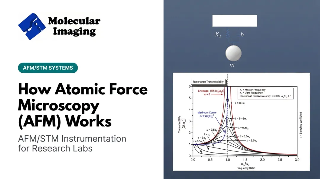
An atomic force microscope maps a surface by feeling it with a sharp probe, then converting that mechanical interaction into a height image. Three subsystems make this possible: the cantilever and tip, the deflection sensor and scanners, and a real-time feedback loop.
The Cantilever and Tip
Every AFM centers on a flexible cantilever tipped with a nanoscale-sharp point, usually silicon or silicon nitride. As the tip nears a sample, short-range forces such as van der Waals interactions cause the cantilever to bend or shift its oscillation. Specialized modes can also engage electrostatic or magnetic forces. That tiny mechanical response, often measured in nanonewtons, is the raw signal an AFM builds into an image.
From Deflection to Data
Most systems detect that response with an optical lever. A laser reflects off the back of the cantilever onto a position-sensitive photodetector, translating minute deflections into an electrical signal sensitive to fractions of a nanometer. Some specialized instruments skip the laser entirely, using fiber-optic interferometry or self-sensing quartz tuning-fork (qPlus) sensors instead. These alternatives suit setups where stray laser light would interfere with the sample or the measurement itself.
With the deflection signal in hand, piezoelectric actuators handle positioning. These ceramic elements expand and contract with applied voltage, moving the tip or sample across the x, y, and z axes with sub-nanometer precision, far finer than any mechanical stage could achieve.
The Feedback Loop That Builds the Image
An electronic feedback loop ties everything together. As the tip scans line by line, the system continuously adjusts vertical position to hold cantilever deflection, or oscillation amplitude in tapping mode, at a constant setpoint. Every micro-adjustment gets logged as a data point tied to an x-y coordinate.
Stitch thousands of those points together and you get a pseudocolor 3D map, where color represents height.

Scanning faster raises tip-sample force and can blur fine detail. Dedicated high-speed AFM systems accept that tradeoff when researchers need to watch a process unfold in real time rather than capture a single static frame.
AFM Imaging Modes Explained
Choosing the right imaging mode comes down to two questions: how much force can the sample tolerate, and what property do you actually need to measure?
| Mode | How it works | Best for |
|---|---|---|
| Contact | Tip stays in constant contact; feedback tracks deflection | Rigid, hard samples; fast scans |
| Tapping (intermittent contact) | Cantilever oscillates near resonance, touching briefly each cycle | Soft or loosely bound samples; general-purpose imaging |
| Non-contact | Tip hovers above the surface, sensing attractive forces only | Fragile biological samples, thin films where contact risks damage |
Contact mode is simple and fast, but dragging a tip across a soft polymer or a loosely adhered protein can smear or displace it.
Tapping mode solves much of that by lifting the tip off the surface between touches, cutting lateral drag. It has become a default choice for ambient and liquid imaging. Contact mode still holds up well on hard, stable materials like metals or ceramics where speed matters more than gentleness.
Non-contact mode goes further for the most delicate samples, sensing only long-range attractive forces without ever touching the surface. The tradeoff is a weaker signal that demands more careful tuning.
Specialized Modes for Property Mapping
Beyond topography, several AFM variants map other physical properties on the same basic platform:
- Magnetic Force Microscopy (MFM): maps magnetic domain patterns, such as on hard disk platters
- Kelvin Probe Force Microscopy (KPFM): measures surface potential and work function, common in semiconductor and battery research
- Electrostatic Force Microscopy (EFM): maps local electrostatic forces and charge distribution on insulating and semiconducting surfaces
- Piezoresponse Force Microscopy (PFM): applies AC bias to map ferroelectric domains and electromechanical response
- Conductive AFM (C-AFM): measures local current alongside topography to reveal conductive pathways and defects
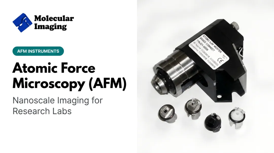
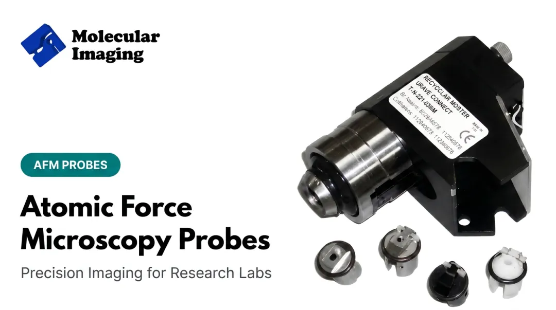
Molecular Imaging's cantilever lineup maps to these modes directly. Dedicated MFM-10, EFM-10 (for EFM and KPFM), and conductive CSAFM probes swap into the same modular nose cone on 5500-series systems.
Key Applications of AFM Across Research Fields
AFM spans many research fields because it measures more than topography—mechanical, electrical, and chemical properties at the nanoscale.
Materials Science and Nanotechnology
Researchers use AFM to characterize polymers, thin films, and 2D materials like graphene for roughness, defects, and crystalline phase boundaries.
Typical targets include:
- Surface roughness and defect mapping on thin films
- Phase boundaries in polymers and composites
- Subsurface structure in multilayer 2D materials
A 2023 contact-resonance AFM study resolved three distinct subsurface regions in oxygen-intercalated multilayer graphene—features hidden just beneath the surface, imaged without damage.
Life Sciences and Bio-Imaging
In liquid, AFM images proteins, cell membranes, and biomolecules without fixing or staining.
Molecular Imaging's 5500 ILM PicoPlus BioAFM uses Magnetic AC (MAC) Mode to image ferritin and DNA nanogrids directly in water. The approach preserves native structure while resolving individual particles at sub-angstrom lateral and 0.2 nm vertical resolution.
Energy and Electrochemistry Research
Energy research is one of AFM's fastest-growing application areas. Conductive and Kelvin probe modes let researchers study battery electrode surfaces and solid-electrolyte interphase (SEI) layers in situ.
What these modes make possible:
- In-situ SEI growth and morphology on electrode surfaces
- Local mechanical contrast (soft organic vs. stiff inorganic layers)
- Edge-plane vs. basal-plane differences tied to degradation
A 2023 operando study combining electrochemical AFM with nano-rheology found graphite SEI forms a soft-organic, stiff-inorganic multilayer at edge planes, but a more uniform mixed layer on basal planes. Platforms like the PicoPlus 5500 series pair conductive contact cantilevers with Kelvin Force Microscope configurations for this kind of in-situ work.
Semiconductor and Molecular Electronics
Conductive AFM captures topography and electrical data at once, so researchers can separate substrate-driven charge injection from probe-contact effects in organic semiconductors.
Conductive AFM configurations can characterize ohmic contacts through nearly insulating molecular junctions.

Advantages and Limitations of AFM
AFM stands out when you need quantitative surface data under real sample conditions—without coatings, vacuum constraints, or conductive substrates.
Advantages:
- Delivers true 3D quantitative height data, not just a shaded 2D impression
- Requires minimal sample preparation
- Operates in air, vacuum, or liquid, including live biological samples
- Measures mechanical, electrical, and magnetic properties, not just shape
Limitations:
- Smaller scan area and slower imaging than SEM—a 2025 comparison notes SEM images in seconds versus several minutes for standard AFM
- Sensitive to thermal drift, tip wear, and artifacts from tip geometry that can broaden fine features
- Faster scanning generally raises tip-sample force and can degrade image quality
What Does an AFM System Cost?
Those tradeoffs shape what you should budget for. Price depends on platform type (research-grade versus benchtop), accessories such as environmental isolation chambers or specialized probes, and whether you need a full system, an expansion, or repair support.
A single average price misleads more than it helps. Request a configuration-specific quote tied to your scan range, imaging modes, and environmental control needs.
Selecting and Maintaining the Right AFM System
Buying or upgrading an AFM system isn't just about specs on a datasheet. A few practical factors matter more over the life of the instrument:
- Modularity: Can nose cones, scanners, or probes swap out to add new modes (KPFM, MFM, C-AFM) later without replacing the whole platform?
- Software compatibility: Will the controller and software still receive support in five or ten years?
- Environmental accessories: Does the system support temperature-controlled stages (often spanning -30°C to 250°C) or isolation chambers for humidity and gas control?
Those same questions matter after install: long-term support decides whether a capable instrument stays productive or sits idle.
Keeping Legacy Systems Running
Many labs still run Agilent or Molecular Imaging platforms like the 5500 PicoPlus, 4500 PicoSTM, or MAC III. These systems were effectively orphaned when Keysight Technologies exited the AFM market in 2018.
They were built well and often remain fully capable, but they need specialized parts, calibration samples, and technicians who actually understand the platform.
That's the gap ZoomAFM fills. Former Molecular Imaging engineers who supported these exact systems from the start offer diagnostics, platform-matched parts, calibration, and remote video support, often without an on-site visit.

When evaluating a new system or a repair partner, prioritize vendors with real technical documentation, video tutorials, and fast remote support. Downtime on a shared instrumentation core facility costs everyone time, not just the researcher whose sample is stuck mid-scan.
Frequently Asked Questions
What is atomic force microscopy?
AFM is a scanning probe technique that uses a sharp cantilever tip to physically sense a surface, mapping topography and other properties at near-atomic resolution without lenses or light.
Is AFM the same as scanning probe microscopy (SPM)?
No. SPM is the broader family of probe-based techniques. AFM is one specific member, alongside STM, MFM, KPFM, and others.
How much does atomic force microscopy cost?
Pricing depends on system type, accessories, and whether you need new equipment, an upgrade, or a repair. Contact Molecular Imaging for a configuration-based quote.
What is the difference between AFM and SEM?
AFM produces true 3D topography in air, vacuum, or liquid without conductive coating. SEM offers faster, larger-area 2D imaging but typically requires a vacuum.
What are the main AFM imaging modes?
Contact, tapping, and non-contact are the three core modes. Tapping mode is the most common general-purpose choice for ambient and liquid imaging.
Can AFM image biological samples in liquid environments?
Yes. Tapping mode and specialized options such as MAC Mode allow imaging of live cells, proteins, and membranes directly in their native liquid state without fixing or staining.