Yet many labs struggle with the same three problems: the instrumentation feels complex, the data channels are hard to interpret correctly, and picking the right system or imaging mode for a given sample feels like guesswork. According to NIST, AFM can achieve subnanometer imaging resolution, while conventional optical microscopy is limited to a few hundred nanometers — a gap that explains why AFM adoption keeps growing across materials science and life sciences.
This manual walks through AFM fundamentals, hardware, imaging modes, data interpretation, applications, and how to choose and maintain a system.
Key Takeaways
- AFM measures surface forces with a cantilever and tip, producing topography without optical resolution limits
- Mode selection (contact, tapping, non-contact) depends on sample hardness and environment
- Height, phase, and amplitude channels report different sample properties; confusing them leads to bad conclusions
- Modular systems and dependable repair support cut research downtime
What Is Atomic Force Microscopy and How Does It Work?
AFM is a scanning probe microscopy (SPM) technique. A sharp tip mounted on a flexible cantilever detects forces near a sample surface—commonly van der Waals forces—though the exact interaction depends on mode, environment, and tip geometry, as described by NIST.
Here's how the feedback loop works, step by step:
- The tip rasters across the sample in x and y while piezoelectric actuators control z-height.
- A laser reflects off the cantilever onto a four-quadrant position-sensitive photodiode (PSPD).
- The controller reads deflection (contact mode) or oscillation amplitude (tapping mode).
- Feedback adjusts the z-piezo to maintain a setpoint.
- That z-correction becomes the topographic image.
Tip sharpness is critical. General AFM tips have radii around 5-20 nm, though specialized high-speed AFM probes can reach apex diameters below 4 nm. A duller tip blurs fine features. This is the root cause of most resolution complaints.

Key AFM Hardware Components
The core hardware stack includes:
- Cantilever/probe — converts tip-sample force into bending or torsion
- Laser + PSPD — optical-lever detection of cantilever motion
- Piezoelectric scanner — precise raster and z-approach motion
- Controller/feedback loop — maintains setpoint, generates height data
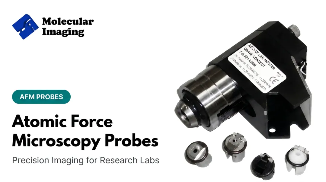
Molecular Imaging's product line reflects this modularity directly. The Pendulum Multipurpose Scanner, used across the 5420 PicoAFM and 5500 PicoPlus families, offers scan ranges from 9 μm × 9 μm for atomic resolution up to 90 μm × 90 μm for broader surveys. Interchangeable nose cones let researchers switch between AFM, STM, conductive AFM, and MFM configurations without buying a new instrument.

Understanding AFM Imaging Modes
Choosing a mode is really about matching tip-sample contact to what your sample can tolerate.
Contact Mode
The tip stays in continuous contact while feedback regulates deflection. It's straightforward and can run fast, but lateral friction can scratch soft samples or dull the probe. Best for: hard, robust surfaces where speed matters.
Molecular Imaging offers dedicated contact cantilevers for this: the ContSi-10 silicon cantilever and the S3N4-10 silicon nitride version, plus a conductive contact cantilever for simultaneous topography and electrical mapping.
Tapping Mode
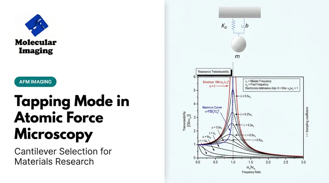
The cantilever oscillates near resonance, touching the surface intermittently. This reduces the lateral drag that damages fragile samples, which is why it's the most widely used mode today. Options in this category include the NCH-30-10 (high frequency), NCL-30-10 (mid frequency), and the softer FM-10 for delicate materials.
Non-Contact Mode
The tip stays in the attractive region of the interaction curve without touching the surface at all. Damage is minimal, but ambient water-meniscus effects can destabilize imaging in air.
Quick mode-selection guide:
| Sample type | Environment | Recommended mode |
|---|---|---|
| Hard, robust materials | Air | Contact |
| Soft polymers, biomolecules | Air or liquid | Tapping |
| Delicate, damage-prone surfaces | Ambient air | Non-contact |
| Biological samples | Liquid | Tapping (BioAFM) |

Specialized variants such as conductive AFM, electrochemical AFM, and BioAFM extend these fundamentals into electrical, in-situ, and liquid-based research. Conductive AFM, for instance, adds electrical mapping on top of standard topography.
How to Interpret AFM Data
Getting good images is only half the job. Reading them correctly is the other half.
The three primary channels:
- Height/topography — actual surface shape, shaped by tip geometry and feedback response
- Phase — contrast from stiffness or chemical differences, not height
- Amplitude — feedback/oscillation response; always interpret alongside drive and setpoint, never alone
In polymer studies, darker phase regions often map to softer, lower-modulus domains (polymer AFM research).
Force curves add another dimension. Measuring cantilever deflection as the tip approaches and retracts lets you extract adhesion, stiffness, and local mechanical properties. One protein study used this approach to measure norovirus particles with z-profiles around 38 nm.
Watching for Artifacts
Three artifacts trip up most new AFM users:
- Tip convolution — features appear broadened or distorted by probe shape, not the sample itself
- Scanner drift — thermal or mechanical motion during a scan, worse in slow-scan directions
- Noise/vibration — from calibration error, piezo creep, or environmental vibration
Before trusting any feature as "real," compare trace and retrace scans, check against a reference sample, and inspect raw line data. Basic processing steps like flattening and plane correction should happen before any quantitative analysis.

Common Applications of AFM Across Research Fields
AFM's versatility shows up across very different disciplines.
Materials science: Thin film and polymer characterization benefit from phase contrast. Research on polypropylene crystallization used AFM to capture transient "dots" during nucleation: ephemeral crystal embryos that other techniques miss entirely.
Life sciences: BioAFM imaging of membrane proteins in native, liquid conditions has achieved roughly 1 nm spatial resolution, according to a biochemistry review on AFM in membrane biology. Molecular Imaging's 5500 ILM PicoPlus BioAFM supports this kind of work directly, with documented applications in endothelial cells, chromatin, sperm cells, and DNA nanogrids.

Electrochemistry and molecular electronics: In-situ and operando EC-AFM tracks battery electrode evolution (morphology changes, cracking, and SEI formation) under live electrochemical control. Molecular Imaging's platforms support this through liquid-cell configurations built for corrosion studies, electrode materials, and fuel cell research.
Choosing and Maintaining Your AFM/STM System
Picking a system comes down to matching modularity and environmental range to your actual research needs, not chasing a single resolution spec.
Factors to weigh:
- Can the scanner switch between AFM, STM, and specialty modes without a full teardown?
- Does the environmental range cover your temperature or humidity needs?
- Is the software compatible with your analysis workflow?
- Are consumables (tips, calibration samples) readily available?
Molecular Imaging's modular systems address this with interchangeable nose cones and scanners, plus environmental control accessories. Temperature stages cover -30°C to 250°C (-22°F to 482°F), with isolation chambers for humidity and gas control and liquid cells for aqueous or solvent-based work.
The web store stocks calibration grids, mica and gold-on-mica substrates, and cantilevers for contact, tapping, liquid, and conductive work.
Regular calibration and probe replacement matter more than most researchers assume. NIST notes that traceable stiffness standards for AFM remain incomplete, so there is no universal calibration schedule. Verify before quantitative work and after any significant change to the setup.
For labs running an aging or malfunctioning instrument, ZoomAFM offers remote diagnostic support for Agilent 5500 and 4500 systems and other Agilent AFM/STM platforms. Coverage includes hardware repair, software troubleshooting, calibration, and preventive maintenance, often via real-time video consultation instead of shipping the instrument out.
Frequently Asked Questions
What is atomic force microscopy and how does it work?
AFM is a scanning probe technique that uses a cantilever-mounted tip to detect surface forces. A feedback loop adjusts tip-sample distance to maintain a setpoint, and that adjustment becomes the topographic image.
How do I interpret AFM data?
Height shows topography, phase reveals stiffness or chemical contrast, and amplitude reflects feedback response. Always cross-check against reference scans and trace/retrace comparisons before treating a feature as real.
What is the difference between contact and tapping mode AFM?
Contact mode keeps the tip in continuous contact, which is simple but can damage soft samples. Tapping mode oscillates the cantilever and touches intermittently, reducing lateral force and protecting fragile surfaces.
Can AFM be used on biological samples in liquid?
Yes. BioAFM systems, like the 5500 ILM PicoPlus BioAFM, use tapping-based modes such as MAC Mode to image live cells, proteins, and biomolecules directly in liquid environments.
How often should an AFM tip be replaced?
There's no universal schedule — replacement depends on wear, imaging mode, and sample abrasiveness. Requalify against a reference sample regularly and swap tips when image fidelity or force calibration degrades.
What should I do if my AFM system is malfunctioning?
Get a professional evaluation before attempting DIY fixes. Services like ZoomAFM offer remote diagnostics and repair for Agilent AFM/STM systems, often resolving issues without shipping the instrument.