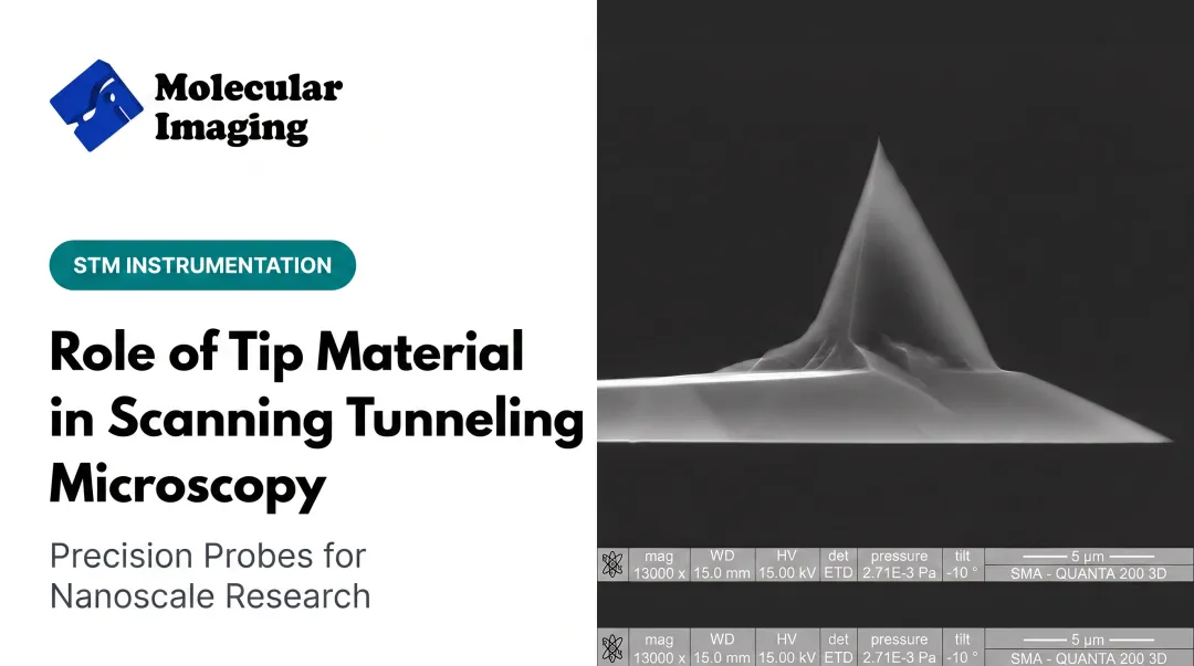
Electrochemical etching of tungsten wire remains the go-to method for producing tips capable of sub-50nm apex radii. But results swing wildly depending on solution strength, applied voltage, cutoff timing, and how deep the wire sits in the etchant. Get one variable wrong, and you're left with a blunt, curved, or unusable point.
This guide walks through whether etching is right for your lab, what you need before starting, the step-by-step process, the parameters that actually matter, and how to troubleshoot when things go sideways.
Key Takeaways
- Sub-50nm apex radius is the standard benchmark for reliable atomic-scale imaging with STM tips
- Cutoff timing matters most: catch the current drop the instant the wire snaps
- Immersion depth of 2-3 mm below the meniscus balances clean breakage against tip deformation
- DIY etching setups with automated cutoff detection can rival commercial machines
- Blunt tips, curved tips, and oxide account for most etching failures
How to Etch Sharp STM Tips
Step 1: Prepare the Wire and Setup
Start with a length of 0.25mm (30 AWG) tungsten wire. Wipe it down with isopropanol to strip away oils from handling; even trace residue can cause uneven etching.
Build your etching cell with both electrodes submerged in etchant:
- Cathode: stainless steel foil or a wire loop
- Anode: your tungsten wire, centered inside the cathode
Before you go further, confirm your jackscrew or Z-stage lowers the wire perpendicular to the solution surface with fine, repeatable control. Sloppy alignment here ruins tips later regardless of how well you dial in voltage.

Step 2: Mix and Position the Etchant
Prepare a 2M sodium hydroxide (NaOH) solution. This is the baseline used in published university protocols and reliably produces sub-50nm tips when paired with proper cutoff timing.
Some labs use potassium hydroxide (KOH) instead, particularly for lamella-loop etching, but NaOH is more common in cutoff-circuit setups.
Position your wire so the tip sits 2-3mm below the meniscus. Check the entry angle: it needs to be perpendicular, or you'll get uneven etching around the circumference.
One quick check before applying voltage: watch for bubbles. They should only form on the cathode. If bubbles appear on the tungsten wire itself, your polarity is reversed. Swap the leads before continuing.
Step 3: Apply Voltage and Monitor Etching
Apply your working voltage. Published protocols vary here: some labs run below 5V, others closer to 9-11V, depending on wire diameter and cell geometry. Start on the lower end and adjust based on test runs with scrap wire.
As etching proceeds, you'll notice tungsten trioxide forming and coating the submerged portion of the wire. This buildup actually helps: it insulates the submerged section and concentrates the etching action at the meniscus, where you want the taper to form.
A full etching cycle typically runs 15-20 minutes, though this depends heavily on wire diameter and solution strength.
Step 4: Trigger Cutoff and Retrieve the Tip
This is the step that separates sharp tips from blunt ones. A current-sensing cutoff circuit needs to detect the sudden current drop the instant the lower wire section snaps off and falls away.
Delay matters more than almost anything else in this process. One well-documented study found that increasing cutoff delay pushed tip radius from roughly 20nm to over 300nm from a fraction-of-a-second lag alone. Faster automated cutoffs (in the microsecond to nanosecond range) have produced tips as sharp as 10nm.

The moment cutoff triggers:
- Withdraw the tip from solution immediately
- Rinse in distilled water or isopropanol
- Inspect under magnification before storage
When Should You Etch Your Own STM Tips?
Etching makes sense when you need consistent, reproducible sub-50nm tips for high-resolution atomic imaging on a regular basis. If your research depends on repeatable results across sessions, an in-house etching setup with a reliable cutoff circuit pays for itself quickly.
Commercial tip-etching machines carry real costs. DIY setups with automated current-sensing cutoffs can deliver comparable sharpness at a fraction of the price.
That said, etching isn't always necessary:
- Basic imaging on atomically flat samples like HOPG often works fine with simple mechanically cut tips
- Without a reliable cutoff circuit, manual timing rarely gets you below 50nm consistently, so you're better off buying pre-made tips
- Labs that image occasionally may find purchasing tips more practical than maintaining an etching rig
What You Need Before Etching STM Tips
Most etching failures trace back to setup problems, not chemistry issues. Before you start, confirm you have the right equipment and materials in place.
Equipment and Materials
- A cutoff circuit capable of detecting rapid current changes the moment the wire separates
- A stable Z-stage or micrometer stage for precise, repeatable control over immersion depth
- High-purity 0.25 mm tungsten wire
- Fresh NaOH or KOH solution mixed to the correct molarity (old solution etches unevenly)
- A stainless steel cathode — foil tube or loop, sized to your etching cell
Safety Readiness
- Wear gloves and eye protection: NaOH and KOH cause severe skin and eye burns on contact
- Work in a ventilated area; etching produces hydrogen gas at the cathode and tungsten trioxide byproduct
- Keep ignition sources away from the cell — hydrogen is flammable
Key Parameters That Affect STM Tip Sharpness
Tip quality comes down to how tightly you control a handful of interacting variables. Loosen your grip on any one of them, and the others can't compensate.
Reference Voltage / Cutoff Sensitivity
This setting controls how fast your circuit shuts off power once the wire breaks. Set the reference close to the actual load voltage at drop-off, and you get the sharpest possible tips. Set it too low, and lag builds in—enough to blunt the point even when everything else is dialed in correctly.
Etchant Concentration
Concentration governs etch rate and how cleanly the wire separates at the meniscus. Too dilute, and etching drags on far longer than necessary. Too concentrated, and you risk rough, uneven etching around the wire.
Wire Immersion Depth
Immersion depth controls how much wire weight hangs below the meniscus, creating the tension needed for a clean break. Too shallow, and the wire may never break at all. Too deep, and excess weight produces a rebound effect: the tip curves or deforms as it snaps free. In comparative tests, shifting immersion from 2 mm to 3 mm moved measured tip radius from roughly 330 nm to 456 nm, depending on cell geometry.

Wire Alignment (Perpendicularity)
An uneven entry angle causes asymmetric etching around the wire's circumference. Even with voltage and depth set correctly, misalignment alone can leave you with a lopsided or blunt tip.
Common Mistakes When Etching STM Tips
Watch for these pitfalls. They account for the majority of failed etches:
- Setting the cutoff reference voltage too far from the actual drop voltage. This is the single biggest cause of blunt tips.
- Restarting the circuit during the kick-start phase right as the tip drops almost guarantees a ruined result.
- Leaving etched tips exposed to air for extended periods lets oxide layers build up before use.
- Skipping depth calibration on scrap wire before etching a real tip leads to failed breaks or rebound curves.
Troubleshooting Issues While Etching STM Tips
Most problems trace back to circuit timing, solution condition, or mechanical alignment. Here's how to diagnose the common ones:
| Problem | Likely Cause | What to Check |
|---|---|---|
| Tip comes out blunt despite cutoff circuit | Reference voltage set too low relative to actual drop voltage | Recalibrate reference closer to observed drop voltage on test runs |
| Wire never breaks | Insufficient immersion depth | Increase depth incrementally to 2-3 mm; confirm perpendicular alignment |
| Tip shows visible curve under SEM | Rebound effect from excess immersion weight | Reduce immersion depth; ensure wire enters straight |
| Bubbles forming on the wire, not the cathode | Reversed polarity | Swap wire connections between cathode and tip lead |
Alternatives to Electrochemical Etching
Etching isn't mandatory for every imaging task. Depending on your sample and resolution needs, other options may serve you better.
Mechanical Cutting with Pliers/Wire Cutters
When it's better: Quick, low-cost tips that work fine for atomic resolution on flat samples like HOPG.
Trade-offs: Inconsistent results and lower yield of usable tips. Performance drops on rougher, non-flat surfaces.
Platinum-Iridium Wire Tips
When it's better: Better oxidation resistance and easier mechanical cutting compared to tungsten.
Trade-offs: The softer material deforms more easily under repeated use.
If you want Pt-Ir without cutting in-house, Molecular Imaging's web store carries ready-to-use etched Pt-Ir and insulated Pt-Ir PT-10 tips. Insulated versions suit electrochemical STM and localized spectroscopy, where tunneling-current control matters as much as sharpness.
Purchasing Commercial Pre-Etched Tips or Professional Instrument Support
When it's better: Labs that want consistent turnaround without building in-house etching capability, or that need repair and calibration support for existing AFM/STM systems.
Molecular Imaging supplies technical documentation, parts, and ZoomAFM diagnostic and repair support for research-grade STM/AFM platforms.
Trade-offs: Higher per-tip cost and less flexibility to customize geometry for specific experiments.
Conclusion
Electrochemical etching, done with tight control over cutoff timing, immersion depth, and solution concentration, reliably delivers STM tips sharp enough for atomic-resolution imaging. Most failed etches stem from a miscalibrated cutoff circuit or incorrect wire immersion depth, not from bad chemistry.
If you're weighing in-house etching against buying pre-made tips, factor in how often you need fresh tips and whether your lab has the bandwidth to maintain a reliable cutoff setup. Researchers who need dependable, high-resolution imaging without the etching learning curve can source etched Pt-Ir tips and instrument support from Molecular Imaging.
Frequently Asked Questions
What solution is best for etching tungsten STM tips?
2M NaOH is the most common choice, especially in setups using automated cutoff circuits. KOH solutions are also used, particularly in lamella-etching techniques.
How sharp does an STM tip need to be for atomic resolution?
A radius of curvature under 50nm at the apex is the common benchmark. Sharper tips (down to 8-10nm) have been demonstrated in published research for the highest-resolution imaging.
Why does etching happen faster at the liquid's surface?
Tungsten trioxide byproduct sinks and coats the submerged wire, insulating it. This concentrates the etching action at the meniscus, where the taper actually forms.
Can I make STM tips without a cutoff circuit?
Manual methods like cutting with pliers can work for basic imaging on flat samples. They rarely match the consistent sharpness that an automated cutoff circuit delivers.
How do I store etched STM tips to prevent oxidation?
Store tips in a sealed container, ideally resting on soft foam submerged in acetone or isopropanol, to limit oxygen exposure. Clean before use regardless of storage method.
What causes a curved or deformed tip after etching?
This "rebound" effect happens when the wire is immersed too deep. The excess weight below the breaking point causes the tip to snap back and deform during separation.