Introduction
The probe is the smallest part of a scanning probe microscope, and it's also the part that determines everything else. A dull or damaged tip can turn a promising sample into a blurry mess, no matter how expensive the instrument driving it.
Many researchers struggle to match the right probe to their AFM, STM, or BioAFM application. Pick the wrong cantilever stiffness or tip coating, and you risk poor resolution, damaged samples, or hours of wasted scan time.
This guide breaks down what SPM probes actually are, the main types you'll encounter, how they function, and how to choose one that fits your research instead of fighting against it.
Key Takeaways
- The probe tip's apex radius, often just a few nanometers, directly sets your image resolution
- AFM cantilevers and STM wire tips work on completely different physical principles (force vs. tunneling current)
- Probe choice depends on imaging mode, sample hardness, and environment (air, vacuum, or liquid)
- Tips wear down with use and need periodic replacement to maintain data quality
- Specialized coatings extend the probe to magnetic, electrical, and chemical mapping beyond basic topography
What Is a Scanning Probe Microscope?
A scanning probe microscope doesn't use lenses or light. Instead, it scans a sharp physical probe across a surface, building an image one pixel at a time. This is what allows SPM techniques to resolve features far smaller than any optical microscope can see.
Atomic force microscopy (AFM) and scanning tunneling microscopy (STM) are the two most common SPM techniques, but they measure completely different signals:
- AFM detects the force between the tip and sample through cantilever deflection, and works on both conducting and insulating materials
- STM measures a tunneling current that flows when a conductive tip sits within a fraction of a nanometer of a conductive surface

Both approaches, according to NIST's overview of scanning probe instruments, rely on a feedback loop that keeps the probe at a controlled distance from the surface while recording position data as topography.
SPM has become a workhorse across nanotechnology, materials science, and life sciences. But every one of those applications depends on the same tiny component: the probe itself.
What Are Scanning Probe Microscope Probes? (Anatomy & Function)
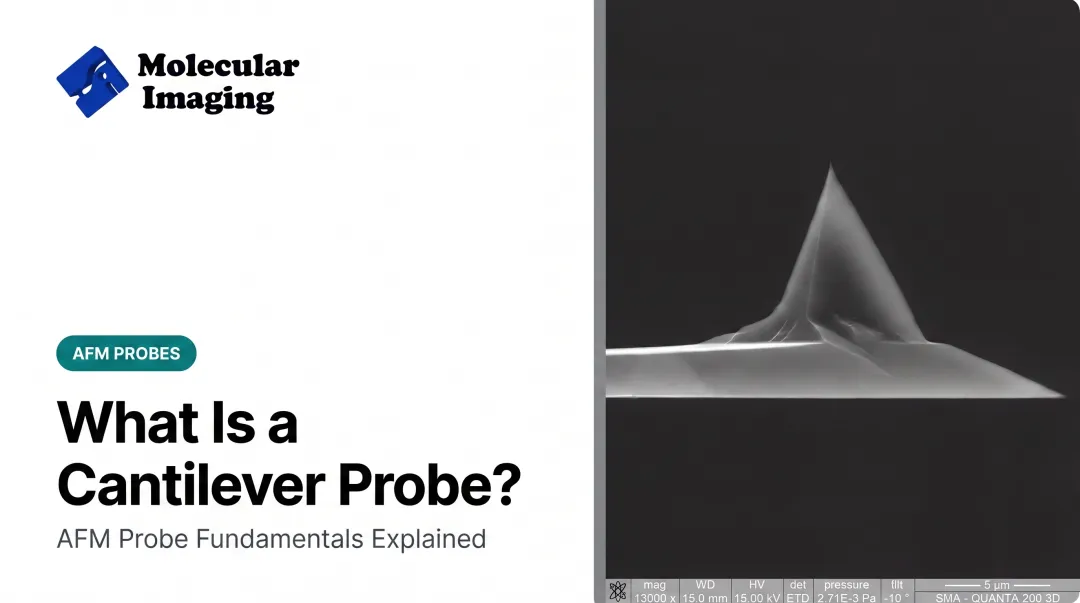
An SPM probe is the sharp physical tip that touches, or nearly touches, the sample surface. In AFM, that tip sits at the free end of a flexible cantilever. In STM, the entire probe is typically a sharpened conductive wire.
Cantilever Mechanics Matter as Much as the Tip
For AFM, the cantilever's spring constant and resonance frequency determine how it responds to surface forces:
- Low spring constant (soft cantilevers) suit delicate, low-force contact imaging
- High spring constant (stiff cantilevers) suit tapping and non-contact modes on hard surfaces
- Resonance frequency governs how fast and stable dynamic imaging can be
These aren't universal numbers. NanoWorld's CONT contact-mode probe is rated around 0.2 N/m and 13 kHz, while Bruker's RTESPA-300 tapping probe runs closer to 40 N/m and 300 kHz. Same category of tool, very different mechanics.
Tip Apex Radius Sets Your Resolution Ceiling
The sharper the apex, the finer the lateral detail you can resolve. A blunt tip physically can't trace a narrow groove or small nanoparticle accurately, no matter how good your electronics are.
Apex quality feeds directly into the feedback loop. Whether the controller tracks cantilever deflection, oscillation amplitude, or tunneling current, that signal is measured continuously and used to adjust probe-sample distance in real time.
A worn or contaminated tip distorts the signal, and a distorted signal means distorted topography. Probe consistency is the difference between a publishable dataset and a re-scan.
Types of Scanning Probe Microscope Probes
Not all probes are built for the same job. Choosing the wrong category often causes more imaging problems than choosing the wrong scan settings.
AFM Cantilever Probes
Standard AFM cantilevers are typically silicon or silicon nitride, fabricated for one of three modes:
- Contact mode: soft, low spring constant cantilevers for continuous tip-sample contact
- Tapping mode: stiffer, higher-frequency cantilevers that oscillate near resonance
- Non-contact mode: similar stiffness to tapping, but operated at greater tip-sample separation
Molecular Imaging's web store carries this full range:
- Contact Mode Silicon Cantilever ContSi-10
- High Frequency Tapping Cantilever NCH-30-10
- Low Frequency Soft Tapping Cantilever FM-10 for gentler sample interaction
STM Tips
STM tips are conductive metal, most commonly etched tungsten or cut platinum-iridium (Pt-Ir) wire. Pt-Ir is a popular first choice for ambient, high-resolution work because the alloy resists oxidation better than tungsten.
Molecular Imaging offers etched and insulated Pt-Ir STM tips (the PT-10 series). The insulated variant minimizes stray current during electrochemical measurements.
Specialized Functionalized Probes
Beyond plain topography, coated probes measure specific physical properties:
- Conductive AFM probes map current alongside height
- MFM probes carry a magnetic coating to image magnetic domains
- KPFM/EFM probes map surface potential and electrostatic force
Molecular Imaging's MFM-10 and EFM-10 (EFM/KFM tapping) cantilevers cover magnetic and electrostatic mapping in this category.
BioAFM Probes
Live cells, proteins, and biomolecules can't tolerate stiff, high-force cantilevers. BioAFM probes use very low spring constants, designed for operation in liquid. Molecular Imaging's Liquid Tapping Cantilever Si-L-10 images soft biological samples in aqueous or physiological conditions without crushing them.
How Sharp Is Sharp?
Tip radius varies far more than most people expect. NanoWorld's SSS-NCH super-sharp silicon probe has a typical radius of just 2 nm. A standard Bruker DNP-10 silicon nitride probe carries a nominal radius of 20 nm, up to 60 nm maximum.
That tenfold gap in sharpness between two common commercial tips is why lateral resolution can swing so widely between setups.

How to Choose the Right SPM Probe
Probe selection comes down to four practical questions: what mode, what sample and environment, what tip geometry and coating, and how long the tip needs to last.
1. Match the probe to your imaging mode. Contact mode needs soft, low-stiffness cantilevers. Tapping and non-contact modes need stiffer cantilevers tuned to a specific resonance frequency range.
2. Consider your sample and environment.
- Soft biological samples in liquid need low-force BioAFM cantilevers.
- Hard materials or conductive surfaces need stiffer or conductive-coated tips.
- Electrochemistry work in solution often calls for insulated STM tips.
3. Evaluate tip sharpness and coatings. Standard silicon works for general topography. Diamond-coated tips (like Molecular Imaging's Diamond-10) add wear resistance for nanoindentation and hard-material testing. Magnetic or conductive coatings add property mapping beyond height alone.
4. Factor in probe lifespan. Tips wear down with repeated scanning. A 2016 wear study published in Scientific Reports found tip radii on rough surfaces growing from around 18 nm to 36 nm after extended scanning, with visibly reduced resolution afterward.
There's no universal scan count before replacement—it depends on force, surface roughness, and scan distance. When images start looking softer or noisier than usual, check the tip before you blame the electronics.
Researchers running legacy Agilent or Keysight 5500-series systems don't need to replace the whole instrument to keep imaging well.
Molecular Imaging's web store stocks compatible cantilevers, STM tips, and calibration samples for these platforms. ZoomAFM handles remote troubleshooting and calibration when resolution or setup drifts.
Probe Materials and Fabrication
Most AFM cantilevers start as single-crystal silicon or silicon nitride wafers. Manufacturers use photolithography and etching (often a KOH or Bosch-style process) to carve out the cantilever shape and sharpen the tip apex during the same fabrication sequence.
STM tips are made differently:
- Tungsten wire is electrochemically etched in a solution like sodium hydroxide until it tapers to a fine point
- Platinum-iridium wire is more often mechanically cut, since the alloy is comparatively unreactive and holds up well in ambient conditions
Beyond base materials, functionalization extends what a probe can measure:
- A magnetic coating turns a standard cantilever into an MFM probe
- Molecules attached to the tip apex enable single-molecule recognition in chemical-force microscopy, not just plain topography
Coating choice, not just tip geometry, often determines what kind of data you can actually collect.
Applications of Scanning Probe Microscope Probes
Probes do more than capture images. Paired with the right AFM or STM system, they measure electrical, magnetic, and mechanical properties alongside topography.
Materials science and nanotechnology:
- Battery electrode characterization, including solid-electrolyte interphase formation during charge cycles
- Polymer blend and thin-film analysis, tracking phase separation and mechanical heterogeneity
- Semiconductor defect and conductivity mapping
Life sciences:
- Live-cell imaging in physiological liquid conditions
- Protein and DNA structural visualization at nanoscale resolution
- Cell mechanics measurements using force-curve techniques
Electrochemistry and molecular electronics:
- In-situ electrochemical AFM tracking electrode degradation during battery operation
- Simultaneous topographic and electrical measurement in molecular junction research
Molecular Imaging supplies contact and tapping cantilevers, BioAFM probes, and Pt-Ir STM tips for these applications. Labs use them in materials research, biophysics facilities, and glove-box electrochemistry setups.

Frequently Asked Questions
What does "scanning probe microscope" mean?
A scanning probe microscope (SPM) is a family of techniques, including AFM and STM, that scan a surface with a physical probe instead of lenses. Tip-sample interaction produces nanoscale images of topography and other properties.
What is a scanning microscope used for?
Researchers use scanning probe microscopes to image surfaces and measure nanoscale properties such as roughness, elasticity, and conductivity. Common applications include nanotechnology, materials science, and biological research.
What is an AFM tip made of?
Standard AFM tips are silicon or silicon nitride. Specialized applications use coatings such as diamond, conductive metal, or magnetic layers for durability or specific measurements.
How sharp is a scanning probe microscope tip?
Tip radii typically range from about 2 nm for ultra-sharp probes to 20–60 nm for standard silicon nitride tips. Smaller radius generally means higher lateral resolution on fine surface features.
Can AFM or STM probes be reused?
Yes, probes can be reused until the tip wears down or breaks. Wear increases tip radius over time, gradually reducing resolution until replacement is needed.
What is the difference between AFM and STM probes?
AFM probes use a flexible cantilever to measure force interactions and work on conductive or insulating samples. STM probes are conductive tips that measure tunneling current, requiring a conductive sample.