This article examines the core categories of nano probes: scanning probe microscopy (AFM and STM) systems, semiconductor test probes for electrical failure analysis, and optical nanoparticles for bioimaging. You'll learn how each probe class works, where it excels, and how to select the right tool for your research.
Key Takeaways
- Nano probes operate at 1–100 nm scale, enabling atomic-resolution imaging and molecular manipulation
- AFM senses surface forces; STM reads tunneling current; semiconductor and optical probes serve circuits and biology
- Uses range from graphene’s 42 N/m strength tests to defect localization in 5 nm-node chips
- Select by conductivity, resolution needs, environment (air, liquid, vacuum), and measurement type
What Are Nano Probes? Understanding the Basics
Nano probes are devices with functional elements measuring 1–100 nm, the scale defined by the U.S. National Nanotechnology Initiative. At this size, probes interact with individual atoms, molecules, and nanoscale structures directly.
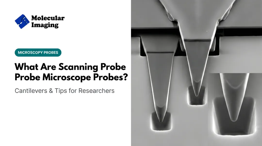
A typical silicon AFM cantilever carries a tip with a 2 nm apex, while tungsten STM tips can be etched to 5.5 nm. These dimensions enable resolution far beyond optical microscopy's diffraction limit.
Two core principles define nano probe operation:
- Close proximity interaction — The probe tip approaches the sample to within a few nanometers or makes gentle contact, creating measurable signals from force, current, or optical interactions.
- Precise positioning — Piezoelectric actuators move the probe in sub-nanometer increments, maintaining controlled separation while scanning across the surface.

Nano probes span both physical tools (AFM cantilevers, STM tips, tungsten semiconductor probes) and functional nanoparticles (quantum dots, gold nanospheres). The distinction matters: a physical probe scans surfaces mechanically or electrically, while optical nanoprobes are distributed inside samples to emit light or scatter signals for imaging.
Historical context: IBM researchers Gerd Binnig and Heinrich Rohrer introduced the scanning tunneling microscope in 1981, using quantum tunneling current to image conductive surfaces at atomic resolution. AFM followed in 1986, extending nanoscale measurement to insulators and biological materials.
Today's specialized probes (conductive AFM, magnetic force microscopy, electrochemical STM) build on this foundation for work in molecular electronics, battery science, and single-cell biology.
Main Types of Nano Probes and Their Applications
Nano probes fall into a few practical families. For surface science and materials labs, AFM and STM probes do most of the day-to-day imaging and measurement work. Other designs serve electrical failure analysis or optical/chemical sensing and are worth knowing mainly for contrast.
AFM and STM Probes
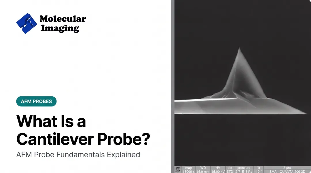
Atomic Force Microscopy (AFM) probes use a flexible cantilever (usually silicon or silicon nitride) with a sharp tip at the free end. As the tip scans a surface, tip–sample forces bend the cantilever. A laser reflects from the cantilever to a photodetector, turning that deflection into topographic maps with sub-nanometer vertical resolution.
Three primary AFM modes:
- Contact mode: Tip stays in steady contact and senses repulsive forces; best on hard, flat samples
- Tapping mode (intermittent contact): Cantilever oscillates near resonance and taps the surface, cutting lateral forces on soft or delicate samples
- Non-contact mode: Tip hovers above the surface and senses attractive van der Waals forces; suited to fragile structures

Scanning Tunneling Microscopy (STM) probes use ultra-sharp conductive tips (often platinum-iridium or tungsten) held within fractions of a nanometer of a conductive sample. Quantum tunneling current flows between tip and surface. That current changes exponentially with distance, so STM can map atomic-scale topography and electronic density.
Specialized AFM variants:
- Conductive AFM (C-AFM): Topography plus local conductivity; maps current paths in nanoelectronics and photovoltaics
- Magnetic Force Microscopy (MFM): Magnetized tips image magnetic domains for media analysis and spintronics
- Kelvin Force Microscopy (KFM/EFM): Surface potential and capacitance maps for semiconductors and organic electronics
- BioAFM probes: Built for liquid imaging of cells, proteins, and DNA at low force
Matching the probe to the mode matters as much as the microscope itself. Molecular Imaging stocks common options for these workflows:
- Contact-mode silicon and silicon-nitride cantilevers
- High-frequency tapping probes (NCH-30-10)
- Liquid-imaging cantilevers (Si-L-10, Si₃N₄-L-10)
- Conductive, MFM-10, and diamond-coated probes for electrical, magnetic, and nanomechanical work
- Etched and insulated platinum-iridium (PT-IR) STM tips for ambient and electrochemical use

Other Nano Probe Categories (Brief Context)
Not every “nanoprobe” is an SPM tip. Two neighboring categories show up often in the literature:
Semiconductor nanoprobes are sharpened tungsten wires (roughly 3–35 nm tip radius) driven inside an SEM for device-level electrical test. Labs use them for MOSFET I–V curves, EBIC junction mapping, and EBAC open/short localization on advanced nodes (example 22 nm SRAM contact probing; 5 nm SRAM transistor work).
Optical and chemical nanoprobes are different tools again. Quantum dots and gold nanoparticles (about 1–15 nm) add fluorescence or plasmonic contrast in bio-imaging (size-tunable QD emission; Au nanoparticle plasmon resonance). Chemical setups such as Nano-DESI and droplet-based sampling probes move femtoliter-to-nanoliter volumes for mass spec or extracellular analysis.
For most AFM/STM users, the decision still comes down to sample type, environment (air vs. liquid), and whether you need topography alone or combined electrical, magnetic, or electrochemical data—and then choosing cantilevers and tips built for that mode.
How Nano Probes Work: Technical Principles
Nano probes work by pairing ultra-fine motion control with a sensor that reads force, current, or light as the tip interacts with the sample. Three technical layers define performance: how the tip moves, what signal it measures, and the environment that keeps that signal stable.
Sub-nanometer positioning: Piezoelectric actuators expand and contract with applied voltage, moving probes at atomic-scale precision. NIST describes scanning at one-to-few-nanometer separation, while commercial systems reach 0.5 nm commanded steps and 0.1 nm resolution under closed-loop control.
Closed-loop systems use position sensors to correct piezo nonlinearity and thermal drift.
Detection mechanisms:
| Probe Type | Signal Measured | Detection Method |
|---|---|---|
| AFM | Cantilever deflection (force) | Laser reflects from cantilever to quadrant photodiode |
| STM | Tunneling current | Constant-current feedback adjusts tip height; constant-height mode maps current |
| Semiconductor | Electrical parameters (I-V, resistance) | Direct current measurement via SEM-integrated probe station |
| Optical | Fluorescence or scattering | Microscope imaging with appropriate excitation and emission filters |
Environmental requirements: Stable data usually depends on the chamber or medium around the probe:
- AFM — Air, liquid cells (aqueous, acid, base, organic solvents), or ultra-high vacuum (UHV); temperature control from -30°C to 250°C
- STM — Conductive samples in ambient conditions or UHV for atomic-resolution imaging; electrochemical cells for in-situ reaction monitoring
- Semiconductor probes — Controlled-atmosphere SEM chambers; prepared device contacts at specific layers
- Optical nanoprobes — Compatible with standard fluorescence microscopes, flow cytometers, or in-vivo imaging systems
When positioning, detection, and environment control sit in one instrument, labs can switch modes without rebuilding the setup. Molecular Imaging's PicoPlus 5500 series integrates AFM, STM, and electrochemical analysis with modular nose cones, with scan ranges from 9 µm × 9 µm for atomic work to 90 µm × 90 µm for larger areas. Top-down and coaxial optical access supports real-time sample observation.
Applications of Nano Probes Across Industries
Nano probes give researchers direct access to mechanical, electrical, and chemical behavior at the nanoscale. Materials labs, semiconductor fabs, biomedical groups, and electrochemistry facilities rely on AFM, STM, and related SPM methods for questions bulk techniques cannot answer.
Materials Science and Nanotechnology
Nano probes measure mechanical properties, surface roughness, grain boundaries, and electronic characteristics of advanced materials at scales where bulk approximations fail.
Graphene stiffness measurement: Lee et al. used nanoindentation on free-standing monolayer graphene, measuring an elastic stiffness of 340 N/m and a breaking strength of 42 N/m. Those values place graphene among the strongest materials per unit thickness. This AFM-based force measurement converted nanoscale deformation into intrinsic mechanical properties that conventional tensile testers cannot obtain.
Additional materials applications:
- Thin films and coatings — AFM quantifies surface roughness of gold-on-mica calibration standards, aluminum oxide films, and diamond-like carbon coatings for semiconductors and data storage
- Carbon nanotubes — Kelvin Force Microscopy maps topography and electrical properties of single-walled nanotubes in polymer composites, showing conductivity variations and contact resistance
- Polymers — Tapping-mode AFM resolves phase separation in blends, crystalline domains, and self-assembled block copolymer patterns
- Nanostructures — STM images atomic steps on graphite, molecular ordering in self-assembled monolayers, and electronic structure of quantum dots

Semiconductor Manufacturing and Electronics
Nano probes localize electrical failures and characterize transistor performance at nodes where feature sizes approach atomic dimensions.
Failure analysis workflow: JEOL's 2024 application note demonstrates transistor I-V characterization, EBIC visualization of pn-junction depletion regions, and EBAC localization of wiring opens and shorts on a 22 nm-node SRAM. Nanoprobing pinpoints defects invisible to optical inspection, enabling targeted circuit redesigns.
Advanced-node capability: Imina reports NMOS and PMOS characterization on a 5 nm-node SRAM die, where traditional probing methods lack the precision to contact nanoscale transistor terminals. Tungsten tips with sub-10 nm radii access individual devices within densely packed layouts.
Quality control impact: Semiconductor manufacturers use nanoprobing to shorten failure-analysis cycles and accelerate root-cause identification when optical inspection cannot resolve the defect.
Life Sciences and Biomedical Research
Nano probes visualize cells, proteins, and biomolecular interactions in their native liquid environments. They expose structures and dynamics that fixed-sample electron microscopy cannot reach.
BioAFM applications: Researchers image bacteria, living cells, and membrane proteins in physiological buffers. High-resolution studies of native and reconstituted membrane proteins show conformational states and assembly dynamics. DNA imaging at liquid-solid interfaces captures double-helix structure, sequence-dependent bending, and protein-DNA binding without dehydration artifacts.
Beyond tip-based imaging, nanoparticle probes serve as optical reporters inside living systems.
Medical imaging potential: Quantum dots enable intracellular and in vivo imaging, traceable drug delivery, and biosensing. Their high brightness and photostability support single-particle tracking and subcellular localization. Gold nanoparticles are being explored for targeted imaging and photothermal therapy, with early clinical safety data emerging.
Theranostics: Theranostic nanoparticles combine diagnostic and therapeutic functions. Quantum dots, for example, can deliver drugs to specific cells while fluorescing to track accumulation. Under light irradiation, they can also generate reactive oxygen species for photodynamic therapy.
Clinical translation caution: A 2024 review found only four quantum dot clinical trials, with concerns about pharmacokinetics, tissue accumulation, heavy metals, and light-induced toxicity. Most optical nanoprobe uses remain investigational.
Electrochemistry and Molecular Electronics
Nano probes enable in-situ monitoring of surface reactions, charge transport at the molecular scale, and battery-electrode evolution during cycling.
Battery research: In-situ electrochemical AFM monitored LiMn₂O₄ cathodes in LiPF₆ organic electrolyte, capturing dissolution and precipitation during charge-discharge cycles through quantitative height distributions. A 2024 Annual Review documents EC-AFM studies of lithium solid-electrolyte interphases, dendrite formation, platinum corrosion, and electrocatalyst dynamics.
Molecular electronics: STM break-junction methods repeatedly form metal-molecule-metal junctions, using the metallic STM tip as one electrode and the substrate as the other. Current-versus-bias measurements across single molecules expose conductance mechanisms, molecular orbital contributions, and electrode-contact effects. That data underpins the design of molecular-scale circuits.
Corrosion and surface chemistry: Electrochemical AFM/STM maps oxide formation, metal dissolution, and self-assembled monolayer organization in real time, connecting nanoscale structure to macroscopic performance.

Selecting the Right Nano Probe for Your Research
Probe choice starts with the measurement, not the catalog. Match mode and tip specs to your sample and environment first, then confirm radius, stiffness, and coatings against your instrument.
Decision framework by measurement type:
| Your Application | Recommended Probe Type | Key Selection Criteria |
|---|---|---|
| Surface topography (any material) | AFM (contact, tapping, or non-contact) | Sample hardness, desired resolution, air vs. liquid |
| Atomic-resolution imaging (conductors) | STM | Sample conductivity, ambient vs. UHV environment |
| Biological / live-cell imaging in liquid | BioAFM (liquid-compatible cantilevers) | Imaging force, resonance frequency in fluid, biocompatibility |
| Conductive mapping | Conductive AFM (C-AFM) or KFM | Current sensitivity, tip coating (metal, doped diamond) |
| Magnetic domain imaging | MFM | Magnetic coating, lift height, sample coercivity |
| In-situ electrochemistry | EC-AFM / EC-STM compatible probes | Chemical resistance, tip insulation, coating stability |
Critical selection parameters:
- Tip radius — Smaller radius improves lateral resolution but may reduce durability. Nanosensors rates super-sharp silicon probes at <5 nm radius (2 nm typical). Bruker groups silicon-nitride tips as sharp (3–10 nm) or medium (11–50 nm).
- Spring constant — Soft cantilevers (0.05–1 N/m) suit force spectroscopy and soft samples; stiff cantilevers (10–100 N/m) work for hard materials and tapping mode in air.
- Conductivity — Mandatory for STM and C-AFM; metal coatings (gold, platinum-iridium, doped diamond) enable electrical measurements.
- Environment compatibility — Verify air, liquid (aqueous, acid, organic), vacuum, and temperature stability from datasheets.
- Resonance frequency — Higher frequencies (200–400 kHz) improve tapping-mode speed and resolution; lower frequencies (10–100 kHz) reduce force in liquid.
Once mode and tip specs are clear, you can source matched cantilevers, STM tips, and standards without trial-and-error ordering.
Molecular Imaging support resources:
- Comprehensive probe catalog — Contact, tapping, liquid, conductive, MFM, KFM/EFM, and diamond-coated cantilevers; etched and insulated platinum-iridium STM tips
- Application guides — Cantilever mounting, amplitude calibration, force-curve analysis, biological sample immobilization, protein imaging, electrochemistry, and MAC Mode operation
- Calibration standards — 500 nm gratings, mica substrates, gold-on-mica reference surfaces for dimensional verification
- Expert consultation — Technical support at 1-888-644-0389 or songxu@nanocuetech.com assists with probe selection, custom system configuration, and troubleshooting
Frequently Asked Questions
What are the main types of nano probes?
The three primary categories are AFM/STM probes (physical cantilevers and tips for scanning probe microscopy), semiconductor nanoprobes (tungsten tips for electrical testing inside SEMs), and optical nanoprobes (fluorescent or plasmonic nanoparticles for bioimaging). AFM probes measure forces; STM probes detect tunneling current; semiconductor probes characterize circuits; optical probes emit or scatter light.
How are nano probes used in medical imaging?
Optical nanoprobes such as quantum dots, gold nanoparticles, and fluorescent molecules add contrast for single-particle tracking and subcellular localization in cells and tissues. Most human uses remain investigational because of clearance, toxicity, and long-term accumulation challenges.
How do nano probes affect the human body?
Medical optical nanoprobes aim for biocompatibility, but safety still depends on composition, coating, size, dose, and route. A 2024 review found only four quantum dot clinical trials, citing heavy-metal and accumulation concerns; gold nanoparticles show early phase I safety without class-wide approval. AFM and STM probes used ex vivo involve no direct human exposure.
From atomic lattices with STM to living cells with BioAFM and chip defects with semiconductor probes, the right tip and system set the resolution you can trust.
Molecular Imaging supplies AFM/STM platforms, cantilevers, STM tips, calibration standards, and ZoomAFM repair support, with documentation and consultation to help you match a probe setup to your research.