Introduction
Atomic force microscopy turned nanoscale imaging from a specialist curiosity into a standard lab technique. Researchers can map surfaces and measure forces at resolutions no optical microscope can touch.
For nearly two decades, the 5500 PicoPlus AFM/SPM has been part of that story. It sits on benches in materials science, life science, and electrochemistry labs across the country.
Keysight Technologies discontinued the platform in 2018, walking away from the AFM market entirely. That left labs holding a working, valuable instrument with nowhere to turn for calibration help, replacement cantilevers, or a straight answer about a firmware quirk.
Many owners now search for basic manuals or a single compatible tip and come up empty.
This guide covers what the 5500 PicoPlus is, how it works, which imaging modes it supports, and where it still fits in current research. It also shows where owners can get manufacturer-level parts and repair support today.
Key Takeaways
- Modular 5500 PicoPlus AFM/STM platform, originally engineered by Molecular Imaging, supports multi-mode nanoscale imaging
- One base unit covers contact, tapping, non-contact, and STM imaging through interchangeable modules
- Used across materials science, life sciences, and electrochemistry research workflows
- Former Molecular Imaging engineers supply parts, repair, and documentation for existing owners
What Is the 5500 PicoPlus AFM/SPM?
The 5500 PicoPlus AFM/SPM is a modular scanning probe microscope that combines atomic force microscopy (AFM) and scanning tunneling microscopy (STM) capabilities in a single interchangeable platform. The "PicoPlus" name marks its tier within Molecular Imaging's product family — a premium, high-performance SPM built for picometer-scale sensitivity, distinguishing it from the more entry-level 5420 PicoAFM in the same catalog. Researchers use it for nanoscale topographic, electrical, and mechanical characterization of both hard materials and soft biological samples. At launch, that range meant one instrument could replace several dedicated microscopes.
Modular by Design
Instead of buying separate instruments for each technique, the 5500 PicoPlus uses interchangeable scanner heads and nose cones. Swap a module, and the same base unit shifts between:
- Standard AFM imaging
- STM
- Current-sensing AFM (CSAFM)
- Kelvin probe force microscopy (KPFM)
- Electrostatic force microscopy (EFM)
- Magnetic force microscopy (MFM) That flexibility is why the platform still shows up in shared instrumentation facilities, where a dozen research groups might each need a different technique from one microscope. The 5500 PicoPlus ships with a dual-range scanner, per Keysight's archived 5500 AFM data sheet:
- Large multipurpose scanner: 90 µm XY and 7 µm Z for broad surface surveys
- Small scanner: 9 µm XY and 2 µm Z for atomic-resolution work
- Small-scanner noise: below 1 Å in XY and under 0.2 Å in Z

Legacy and Evolution of the Agilent 5500 Series
The platform's roots trace back to Molecular Imaging Corporation (MIC), founded by Arizona State University researchers in the early 1990s. Agilent Technologies acquired MIC in November 2005, folding the PicoPlus line into its nanomeasurements portfolio. The product later moved under Keysight Technologies when Agilent spun off its electronic measurement business. Keysight exited the AFM market entirely in 2018, discontinuing the 5500 series and leaving existing owners without a manufacturer to call. A group of former Molecular Imaging engineers, including Dr. Song Xu, revived the company under its original name. That design history is why they can still troubleshoot a twenty-year-old scanner head, source modules and parts, and support labs that kept the 5500 PicoPlus in service.
How Does the 5500 PicoPlus AFM Microscope Work?
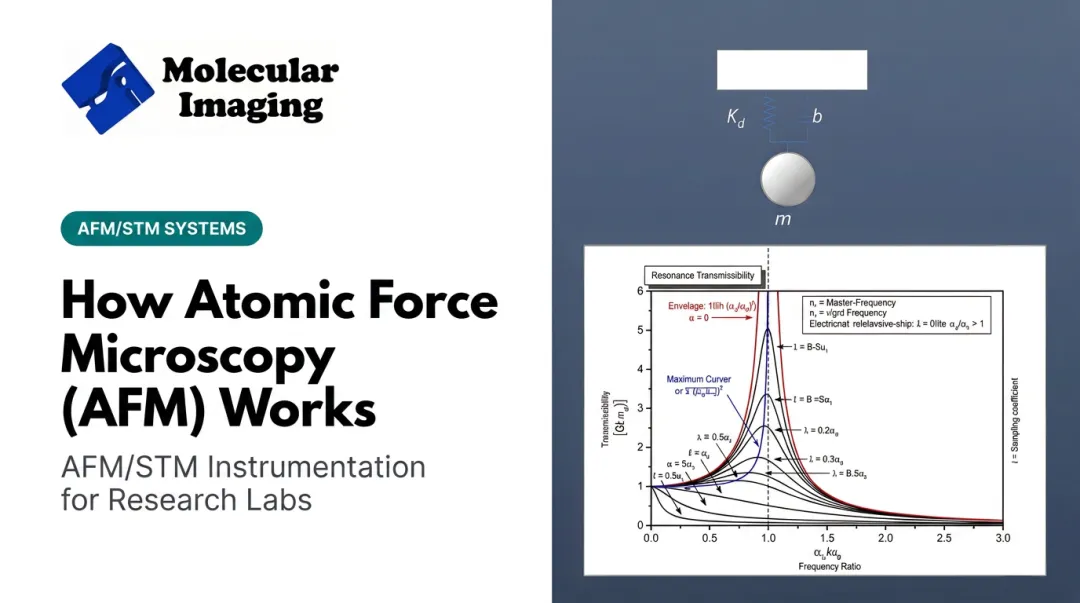
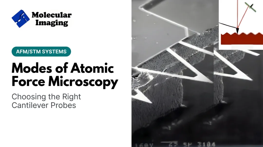
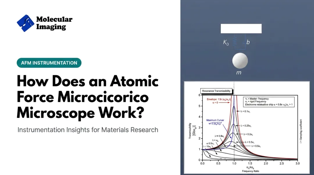
The 5500 PicoPlus works like every optical-lever AFM: a sharp tip mounted on a flexible cantilever scans across the sample surface. As the tip encounters bumps, valleys, or shifts in stiffness, the cantilever bends. A laser reflects off the back of the cantilever onto a position-sensitive photodetector, and even sub-nanometer deflections show up as a measurable shift in the reflected beam.
The Feedback Loop
The system doesn't just record deflection passively. Electronics constantly compare the cantilever's signal against a setpoint and adjust the piezo scanner in real time — pulling the tip back when force gets too high, easing it closer when the signal drops. That correction, repeated thousands of times per line, builds the point-by-point topographic map researchers see on screen.
Movement at this scale relies on a piezoelectric tube scanner. Four external electrodes wrap the tube; differential voltage across opposite quadrants bends it laterally for X-Y motion, while equal voltage across all four quadrants stretches or contracts it axially for Z positioning. That's the mechanism behind the platform's sub-angstrom stability.
Added STM Capability
Swap in the STM nose cone, and the same platform measures something different: tunneling current. A conductive tip approaches a conductive sample within a few atomic diameters, and a small bias voltage produces a quantum tunneling current extremely sensitive to tip-sample distance. In constant-current mode, feedback adjusts tip height to hold that current steady, and the resulting Z-motion becomes the image.
Whether the signal is cantilever deflection or tunneling current, high-performance control electronics translate it into usable data—and software matters just as much. Molecular Imaging continues to support legacy Agilent and Keysight documentation alongside Gwyddion, an open-source SPM analysis platform, giving owners a current path for processing images without discontinued proprietary software.
Beyond the scan head itself, accessories set the conditions the instrument can hold:
- Temperature-controlled stages operating from -30°C to 250°C for phase-transition and thermal studies
- Environmental isolation chambers managing humidity, low-oxygen conditions, and gas composition
Both matter for battery research and reactive-gas studies where ambient air would ruin the experiment.
Imaging Modes: Contact, Tapping, and Beyond
Every AFM technique on the 5500 PicoPlus comes down to how the tip interacts with the surface. Choosing the right mode depends heavily on what the sample can tolerate.
Contact mode keeps the tip in continuous physical contact while the feedback loop regulates cantilever deflection. It's straightforward and reliable on hard, stable materials like metals or crystalline films. The tradeoff: constant lateral dragging can scratch or destroy soft, loosely bound samples.
Tapping mode (intermittent contact) oscillates the cantilever near its resonant frequency so the tip only briefly touches the surface at the bottom of each cycle. Feedback regulates amplitude, phase, or frequency instead of constant deflection. Because lateral drag drops dramatically, tapping mode is the default for:
- Biological samples like proteins, DNA, and cells
- Soft polymers and thin coatings
- Long scans where preserving tip sharpness matters
Those advantages explain why tapping mode dominates bio-AFM work. It protects both the sample and the tip through extended imaging sessions.
Non-contact mode suits samples too delicate or contamination-sensitive for even brief tapping contact. The oscillating tip stays in the attractive-force region above the surface entirely, though ambient humidity can create a water meniscus that interferes with stable operation.
STM and electrical modes enable atomic-resolution tunneling-current imaging for conductive samples. Additional modules cover:
- Current-sensing AFM
- Kelvin probe force microscopy for surface potential mapping
- Magnetic force microscopy for domain imaging on materials like hard drive platters
None of this requires separate instruments. A researcher imaging a polymer blend in tapping mode this morning can switch to STM on a conductive sample this afternoon, using the same base unit and control electronics. That flexibility is a big reason the platform remains popular in shared core facilities.

Applications Across Nanotechnology, Materials Science & Life Sciences
Materials Science & Nanotech R&D
The 5500 PicoPlus has long supported characterization of thin films, polymers, and nanostructures. Documented use cases include:
- Conductivity mapping of TiW films to study grain-boundary effects
- Resistivity imaging of SiGe heterostructures
- Temperature-dependent phase transitions in VO2 films via the temperature-controlled stage
- Block copolymer surface texture changes during toluene vapor exposure and in-situ heating
- STM imaging of fullerene-class molecules on HOPG, resolving individual molecules and their arrangement
Battery research is a growing use case. Paired with the environmental isolation chamber, the platform supports electrode surface characterization under controlled humidity and oxygen conditions. That setup matches the demands of modern in-situ electrochemical battery research that tracks solid-electrolyte-interphase formation.
The same environmental control that enables battery work also opens the door to gentle, in-liquid imaging for biological samples.
Bio-AFM in Life Sciences
Bio-AFM uses tapping mode in liquid to image cells, proteins, and biomolecules without denaturing them. Documented examples include:
- DNA and protein imaging, including hexagonal DNA nanogrid self-assembly and S-layer protein arrangement
- Chromatin structure imaging in aqueous buffer
- Sperm cell and liposome morphology studies
- Drug molecule interaction imaging at the 2-5 nanometer scale
Tapping-mode studies of proteins like lysozyme have captured substrate-dependent height fluctuations as small as 1 nanometer over roughly 50 milliseconds — detail invisible to contact mode or standard microscopy.
Beyond soft-matter and biological imaging, the platform’s in-situ electrochemical modes support real-time surface chemistry work.
Electrochemistry & Molecular Electronics
In-situ electrochemical AFM and STM observe surface reactions as they happen. Documented examples include:
- Copper deposition and crystal growth monitoring during electrochemical reduction
- Cyclic voltammetry of gold surfaces with underpotential deposition peaks near 0.27 V
- Kelvin probe-based corrosion analysis
In molecular electronics, the STM configuration supports single-molecule charge-transport studies, tracking conductance through molecular junctions formed between metal electrodes.

Keeping Your 5500 PicoPlus Running: Parts, Service & Support
Owning a discontinued instrument creates a specific kind of headache. Calibration drifts, a cantilever snaps, or a controller board fails, and there's no manufacturer number to call.
Generic electronics repair shops can fix a circuit board, but they don't understand piezo tube calibration or why a 5500's feedback loop behaves differently from a competitor's system.
This isn't a rare problem. Used and aging lab equipment already makes up roughly 2-3% of global laboratory equipment sales, worth close to $2 billion annually.
One documented case found the nearest repair facility for an aging instrument was more than 2,100 miles away. Shipping alone was cost-prohibitive before repair even began.
ZoomAFM fills that gap. Molecular Imaging operates ZoomAFM, a repair and service line staffed by engineers who worked on the original 5500 platform. Services include:
- Remote diagnostics over video conferencing before any parts ship
- Hardware and software troubleshooting
- Preventive maintenance to catch problems before they cause downtime
- Replacement parts matched to the platform rather than generic substitutes
Molecular Imaging's web store also stocks contact, tapping, and liquid-environment cantilevers, STM tips, calibration grids, and gold-on-mica substrates built for the 5500 series. The site hosts free downloads of legacy Agilent and Keysight manuals, scanner calibration procedures, and wiring schematics. That documentation used to require a support contract to access.
Frequently Asked Questions
What is a PicoPlus AFM and what is it used for?
A PicoPlus AFM is a modular scanning probe microscope platform originally built by Molecular Imaging, combining AFM and STM capability in one instrument. Researchers use it for nanoscale topographic, electrical, and mechanical characterization across materials science, life sciences, and electrochemistry.
How does the PicoPlus AFM microscope work?
A cantilever with a sharp tip scans the sample while a laser reflects off it onto a position-sensitive photodetector that measures deflection. A feedback loop adjusts the piezo scanner in real time to hold constant force or amplitude, building the image point by point.
What is tapping mode on an AFM?
Tapping mode oscillates the cantilever near its resonant frequency so the tip only briefly contacts the surface during each cycle. This reduces lateral drag, protecting soft or fragile samples like proteins, cells, and thin polymer films from damage.
Can I still get parts and service for an Agilent 5500 AFM?
Yes. Molecular Imaging, staffed by former engineers who built the platform, offers cantilevers, calibration samples, and documentation through its web store. Repair and remote diagnostics are available through ZoomAFM.
What is the difference between AFM and STM modes on the 5500 PicoPlus?
AFM measures physical force between a cantilever tip and the sample surface to build a topographic image. STM instead measures tunneling current between a conductive tip and a conductive sample, enabling atomic-resolution imaging of conductive surfaces.
How do I choose the right imaging mode for my sample?
Hard, stable materials generally suit contact mode, while soft or biological samples do better under tapping or non-contact mode. Conductive samples that need atomic resolution call for STM. Each mode swaps in through the platform's modular nose cone.