Introduction
You're hunched over a circuit board, trying to solder a 0603 resistor smaller than a grain of rice. Your chisel tip keeps bridging two pads that sit less than a millimeter apart. Sound familiar?
Tip shape matters just as much as iron temperature, and most people learn this the hard way. Soldering iron tips come in a handful of shapes, but the conical tip is the one you'll see most often — and also the one most misunderstood.
This guide breaks down what conical tips actually are, when they earn their place on your bench, how they stack up against chisel and bevel tips, and how to choose and maintain one so it doesn't wear out in a week.
Key Takeaways
- Conical tips concentrate heat into a small area, ideal for fine SMDs and tight-access soldering
- The cone's side, not just the point, usually does the real work of heat transfer
- They're less efficient on large joints and more fragile under pressure than chisel tips
- Matching tip size to the pad — not always going smaller — is the single biggest factor in performance
What Are Conical Tips?
A conical tip is a probe apex shaped like a cone: wide at the base and tapering to a sharp point. In AFM and STM, that geometry sets how the tip meets the sample, how small a feature you can resolve, and how the probe wears over repeated scans.
Unlike a blunt or worn tip, a well-formed cone presents a small end radius while the shank still has enough bulk for mechanical stability. For labs running contact, tapping, or tunneling measurements, tip shape is as practical a spec as spring constant or coating.
What “Conical” Means on an SPM Probe
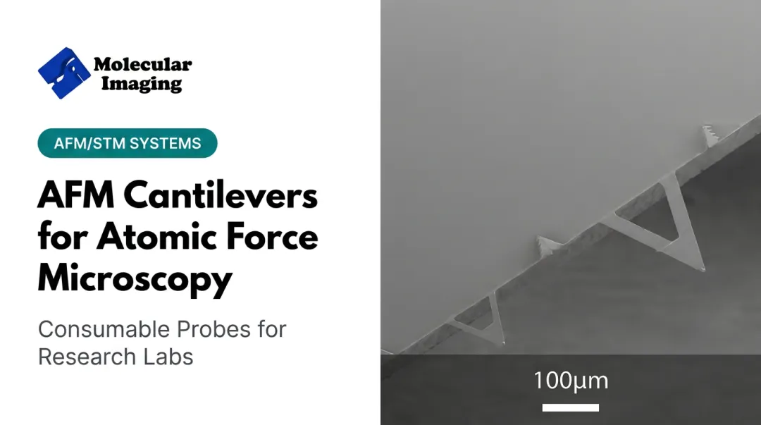
On an AFM cantilever, the sensing tip is often a microfabricated cone or cone-like spike at the end of the lever. On an STM probe, the tip is usually a sharpened metal wire (commonly etched platinum-iridium) whose apex approximates a cone.
Key geometric parameters:
- End radius — smaller radius generally improves lateral resolution on fine features
- Aspect ratio — taller, narrower cones reach into trenches and rough topography with less sidewall averaging
- Cone angle — affects how much of the shank interacts with steep sidewalls
- Tip height — sets clearance above the cantilever or holder for the sample relief you need
Catalog names vary by vendor. Treat “conical,” “sharp,” and “high aspect ratio” as starting labels, then read the stated radius, angle, and height.
Materials and Coatings
Uncoated silicon or silicon-nitride cones are common for standard topography. Conductive coatings support EFM, KFM, and other electrical modes. Hard coatings (including diamond-coated options) trade some tip sharpness for wear resistance on abrasive samples.
For STM, etched PT-IR tips are widely used when you need a conductive, mechanically robust apex for tunneling. Insulated PT-IR variants matter when the experiment requires defined electrochemical or liquid exposure at the very end of the tip.
When Conical Geometry Helps
Conical tips are a strong default when you need a predictable, symmetric apex and straightforward interpretation of images on relatively open surfaces. They suit many materials-science and nanotech workflows where features sit on a flat or gently varying substrate.
High-aspect-ratio cones help more when the surface is rough, porous, or patterned with deep gaps. A blunt or pyramidal tip can still image the top surface, but it may broaden trenches and round sharp corners in the data.
Practical Limits (Not Just the Point)
Resolution is not only “how sharp the point looks.” Tip convolution means the recorded image is always a mix of real sample shape and tip shape. As the cone wears or picks up debris, effective radius grows and fine structure softens even if the instrument is otherwise stable.
Symmetric cones also do not automatically solve every sidewall problem. On near-vertical walls, a finite cone angle still touches the feature before the true apex reaches the bottom. Matching tip geometry to feature depth and angle matters as much as picking the right scan mode.
Common Variants You’ll See
- Standard conical AFM tips — general topography in air; balanced radius and durability
- Sharp / reduced-radius cones — finer lateral detail on delicate or densely featured samples
- High-aspect-ratio cones — deeper access on trenches, grains, and structured films
- Conductive conical probes — electrical and potential modes (EFM/KFM and related)
- Etched PT-IR STM tips — tunneling tips for STM and combined AFM/STM platforms

Molecular Imaging supplies AFM cantilevers across common modes plus etched and insulated PT-IR STM tips for labs that need replacement probes matched to imaging conditions, not only whole-system hardware.
Choose conical geometry when you want a symmetric apex and clear specs for radius and aspect ratio. Move to a specialized tip shape only when your sample’s depth, hardness, or electrical mode demands it.
When to Use Conical Tips: Best Applications
Conical tips shine in situations where precision beats raw heat capacity.
Fine SMDs and Discrete Components
Tiny surface-mount devices, resistors, and diodes are the conical tip's home turf. When you're working on 0603-sized packages or similarly dense boards, a thin conical tip lets you touch exactly one pad without bridging its neighbor.
Tight, Hard-to-Reach Spaces
Wire connector housings, densely packed PCBs, recessed pads — anywhere a chisel or wedge tip physically can't fit, a conical tip usually can. Its narrow profile is the whole point.
Thin Wire and Through-Hole Work
Conical tips generally pair better with smaller-gauge wires than thick cable that needs more thermal mass behind it. They also handle discrete through-hole components with standard lead diameters well, since you're soldering one lead at a time rather than dragging across several.
A word of caution: that sharp, narrow geometry is also the conical tip's weak point. Excess downward force can bend, crack, or wear the tip faster than a broader shape would tolerate. If you're new to soldering, use a light touch — let the heat do the work, not pressure.
Drag Soldering — With Caveats
Some technicians do use conical tips for drag soldering multi-lead SMDs, feeding solder while sliding the tip along a row of pins. It works, but bevel and hoof tips are generally better suited to this task because they hold more solder against the leads. Think of conical drag soldering as a workaround, not the default method.
Conical Tips vs Other Soldering Tip Shapes
Choosing the right shape comes down to matching geometry to the job in front of you.
Chisel Tips
Chisel tips have a broad, flat face — the opposite of a conical tip's pinpoint focus. That wider contact area makes chisels the better all-purpose choice for general wiring and through-hole work, where you need more heat delivered across a bigger joint rather than precision on a single pad.
Bevel & Hoof Tips
Bevel and hoof tips are cut at an angle, which lets them hold and carry more solder. This makes them the preferred shape for drag soldering across multiple leads on SOICs or QFPs. Conical tips can't hold solder the same way, so they're better reserved for single-point contact rather than solder-loaded dragging.
Knife & Blade Tips
Knife and blade tips can contact a joint by point, line, or flat face depending on how you angle them, which makes them useful for rework, solder bridge repair, and multi-lead components. A conical tip's small contact area would be inefficient for clearing a bridge across several pins — the knife's versatility wins there.
| Tip Shape | Best For | Weak Point |
|---|---|---|
| Conical | Fine SMDs, tight spaces, single-point work | Limited thermal mass, easily damaged |
| Chisel | General wiring, through-hole, broad contact | Too big for dense boards |
| Bevel/Hoof | Drag soldering multi-lead packages | Less precise for isolated pads |
| Knife/Blade | Bridge repair, rework, multi-lead access | Overkill for tiny single joints |

Pros and Cons of Conical Tips
Advantages:
- Concentrates heat precisely where you need it
- Reaches tight, crowded, or recessed areas other shapes can't
- Ideal for fine SMD work and thin-gauge wire
- Widely available and generally the lowest-cost "default" tip shape
Limitations:
- Smaller thermal mass means slower heat transfer into larger joints
- Sharp geometry is more prone to damage from excess force or mishandling
- Holds less solder than hoof or bevel tips, making it a poor fit for drag techniques
Before committing to a conical tip over a chisel or bevel alternative, weigh how much precision you actually need against how much abuse the tip will take on your bench.
How to Choose and Care for Conical Tips
Sizing: Match, Don't Minimize
The instinct is to grab the smallest conical tip available for detailed work. Resist it.
A tip that's too small for the joint transfers heat poorly, so you dwell longer and risk overheating the pad. Match the tip to the joint or pad you're working on—not the smallest size on the rack.
Compatibility First
Not all conical tips are universal. Cartridges from Hakko, Weller, PACE, and Metcal are typically built for their own handpiece and station systems. Before buying, confirm the tip is rated for your specific iron. A tip that doesn't seat correctly won't transfer heat properly, regardless of shape.
Maintenance That Actually Extends Tip Life
Metcal's tip care guide recommends these practices:
- Keep the tip tinned during use and storage to limit oxidation
- Use the lowest practical temperature for the job
- Avoid excess pressure — let heat, not force, make the joint
- Clean with a damp sponge or brass wool, never sandpaper or files
- Turn the iron off or drop the temperature when idle
Lead-free solders also wear tips faster than leaded alloys because of higher tin content and more aggressive fluxes. If tips degrade sooner after a lead-free switch, that chemistry is the usual cause, not a defective tip.
Precision at Every Scale: Conical Tips Beyond Electronics
The core idea behind a conical tip — concentrating precision into the smallest possible point — doesn't stop at the soldering bench. The same principle governs instruments working at scales millions of times smaller than a circuit board.
In atomic force microscopy (AFM) and scanning tunneling microscopy (STM), probe tips are engineered in conical or pyramidal shapes for a nearly identical reason: geometry determines the resolution you can achieve. A dull or poorly shaped AFM probe tip produces blurred topography data, much like an oversized soldering tip produces imprecise joints.
At Molecular Imaging, this principle shows up directly in the probe catalog:
- Etched Pt-Ir STM tips, sharpened through an etching process to achieve atomic-scale resolution
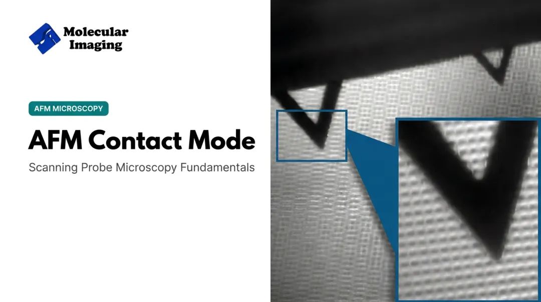
- Silicon and silicon nitride contact-mode cantilevers, built with pyramidal tip geometries for high-resolution topographical imaging
- Diamond-coated indentation cantilevers, preserving a precision tip beneath a wear-resistant coating for nanomechanical testing

Whether you're soldering a resistor or imaging a protein molecule, tip geometry sets the ceiling on precision. Researchers in nanotechnology, materials science, or life-science imaging can explore Molecular Imaging's full range of AFM cantilevers and probe accessories.
Frequently Asked Questions
What is the best shape for soldering tips?
There's no single best shape; it depends on the job. Chisel tips are the most versatile all-purpose choice, while conical tips excel at precision work in tight, crowded spaces.
What is the golden rule of soldering?
Match the tip size and shape to the joint, keep the tip properly tinned, and never force excess pressure onto the work. Heat and contact area do the job, not pressure.
What size is a T18 tip?
T18 refers to a Hakko soldering tip series compatible with specific Hakko iron handpieces like the FX-8801. Exact millimeter dimensions vary by tip within the series, so check Hakko's official product listing for precise sizing.
What is a conical tip used for?
Conical tips are used for precision soldering on small SMDs, fine-gauge wires, and components packed into tightly clustered layouts where larger tips can't fit.
Are conical tips good for beginners?
Beginners can use them, but should be cautious: the sharp point is prone to damage from excessive pressure. A chisel tip may feel more forgiving while you're still building technique.
How do I know if I need a conical soldering tip?
If your work involves tiny components, restricted access, or point-to-point precision rather than high-volume heat transfer into large joints, a conical tip is likely the right call.