Optical microscopes can't resolve it. Electron microscopes often need vacuum and can damage delicate flakes. That's where atomic force microscopy (AFM) has become the default tool in materials labs. It resolves vertical steps well below a nanometer, works in air or liquid, and can measure electrical and mechanical behavior at the same time it maps shape.
This article covers how AFM works, why it fits 2D materials so well, the specific applications researchers rely on, and what to look for when choosing a system.
Key Takeaways
- AFM measures topography at sub-nanometer vertical resolution, letting researchers distinguish single- from multi-layer flakes
- Modes like KPFM, conductive AFM, and friction imaging reveal defects and electrical behavior invisible in plain topography
- Air-sensitive materials like black phosphorus and MXenes need humidity and oxygen control, not just a sharp tip
- Modular AFM/STM platforms let one instrument cover multiple techniques instead of buying separate systems
What Is Atomic Force Microscopy and How Does It Work?
Atomic force microscopy (AFM) is a scanning probe technique that maps surface topography at the nanoscale. It works by scanning a sharp tip, mounted on a flexible cantilever, across a surface. As the tip encounters bumps and valleys, the cantilever bends. A laser reflects off the cantilever onto a photodetector, and that deflection signal is converted into a height map.
A feedback loop keeps the tip-sample force (or oscillation amplitude, depending on mode) constant as the scanner moves. This loop is what produces a clean 3D topography image rather than a crashed tip or a blurry mess.
Two resolution numbers matter here:
- Lateral resolution: typically 2-10 nm, depending on tip sharpness and imaging mode
- Vertical resolution: better than 0.1 nm in many configurations
That vertical number is the whole reason AFM dominates 2D materials work. A graphene sheet is roughly 0.3 to 1 nm thick, well within AFM's detection range. Unlike scanning electron microscopy, AFM doesn't require a vacuum chamber. It runs in air, in liquid, even inside a glovebox, which matters when your sample degrades the moment it touches oxygen.

Why AFM Is the Preferred Tool for Graphene and 2D Materials
Sub-Angstrom Height Resolution on Atomically Thin Samples
Optical microscopy can spot a graphene flake's outline through color contrast on certain substrates, but it can't tell you if you're looking at one layer or five. Electron microscopy images the surface but struggles with true out-of-plane thickness measurement.
AFM measures the actual step height. That said, the numbers aren't as tidy as textbooks suggest. A 2016 study published in Nanotechnology found reported single-layer graphene thickness values ranging from 0.4 to 1.7 nm across the literature, driven by tip-surface interactions, imaging force, and surface contamination.
Humidity matters too. Researchers working with graphene on mica found apparent thickness measured 0.34 nm below 10% relative humidity, versus 0.67 nm at 20% humidity or higher, in a 2019 study in Review of Scientific Instruments.
AFM thickness values are real measurements, but they're study-specific, not universal constants. Calibration matters. Molecular Imaging's 500 nm grating calibration sample is one practical way labs verify scanner accuracy before trusting a graphene height reading.
Multimodal Characterization Beyond Topography
Topography alone misses a lot. A graphene sheet can look flat and uniform while hiding electrical dead zones or mechanical weak points. That's why researchers layer on additional modes:
- Kelvin probe force microscopy (KPFM): maps surface potential and work function, useful for spotting grain boundaries and wrinkles in CVD graphene
- Conductive AFM: measures local current with a biased tip, revealing where a film conducts poorly
- Lateral force microscopy (LFM/friction): picks up domain orientation and layer-dependent friction differences
- Force modulation/nanomechanics: maps stiffness and adhesion, flagging defects and strain
Hardware for these modes is available off the shelf. Molecular Imaging's EFM-10 tapping cantilever supports KPFM-style surface potential work, while its conductive contact cantilever supports conductive AFM for spotting weak conduction paths in imperfect CVD films.

Sample Manipulation and Nanolithography Capability
AFM tips aren't limited to imaging. A biased tip can locally oxidize graphene, using the nanoscale water meniscus between tip and surface as a tiny electrochemical reaction zone.
Researchers used this technique to fabricate graphene/graphene-oxide/graphene junctions, tuning the tip bias to shift the junction from semiconducting toward semi-insulating behavior, as reported in a 2011 Nano Letters study.
This matters for device prototyping. You get residue-free, site-specific patterning without a mask, though line width depends heavily on humidity, load, and layer count. Molecular Imaging's 5500 AFM systems support tip-based lithography, documented for creating nanoscale patterns and even nanografting self-assembled monolayers on gold, alongside standard imaging.
Compatibility with Sensitive Sample Environments
Some 2D materials fall apart the moment they see air. Black phosphorus degrades rapidly with oxygen exposure. MXenes oxidize even under refrigeration if handled outside controlled conditions.
This is why AFM's compact footprint matters as much as its resolution. It fits inside a glovebox.
Molecular Imaging's temperature-controlled stages (-30°C to 250°C) and Environmental Isolation Chambers give labs control over humidity, temperature, low oxygen, and gas composition—the conditions needed for battery electrode research or reactive-gas studies where the sample can't tolerate ambient air.

Key Applications of AFM in Graphene and 2D Materials Research
Measuring Flake Thickness and Layer Count
Height histograms remain a workhorse technique. Researchers scan across a flake edge, plot the height distribution, and count discrete steps corresponding to layer boundaries. Published examples include:
| Sample | Reported AFM thickness |
|---|---|
| 1-, 2-, 4-layer graphene | 1.5, 1.9, 2.73 nm |
| CVD few-layer graphene | 0.7-1.2 nm |
| CVD film grown at 1350-1550°C | 0.7-3.7 nm average |
These figures, compiled in a 2021 focused review, are reference points—not fixed constants. Verify them against your own calibrated measurements.
Evaluating Growth Quality (CVD Graphene)
Chemical vapor deposition graphene rarely comes out perfect. Grain boundaries, wrinkles, and folds show up constantly. Topography alone often misses them.
Pairing complementary AFM modes fills those gaps:
- KPFM resolves distinct work-function signatures at grain boundaries and different wrinkle types
- Conductive AFM adds electrical context; CVD films conduct measurably worse than mechanically exfoliated graphene
- Friction-force imaging reveals twisted top layers and stacking faults invisible in height data alone
Studying Moiré Patterns and Angular Mismatch in Stacked Layers
When two 2D layers stack with a slight rotational offset, they create a moiré superlattice, a periodic pattern with real implications for electronic behavior. Torsional force microscopy, an AFM technique sensitive to dynamic friction, can image these patterns in air without electrical bias.
A 2024 study in PNAS demonstrated this on graphene-hBN stacks, measuring a 2.6 nm moiré period corresponding to a 5.4-degree twist angle, along with examples down to roughly 1-degree mismatch. Researchers calculate the twist angle from the moiré wavelength using the lattice-mismatch relation for the material pair.

Investigating Mechanical and Electrical Properties for Device Design
Combined electrical and mechanical AFM measurements show up across several research areas:
- Battery research: in-situ AFM has visualized solid-electrolyte-interphase formation on graphite electrodes, tracking nucleation near 0.9 V and stabilization near 0.3 V
- Polymer composites: AFM phase imaging reveals how graphene nanofillers distribute and exfoliate within epoxy matrices
- Molecular electronics: combined STM/AFM setups have resolved gate-tunable molecular energy levels on graphene-based device stacks
Across these areas, the shared need is the same: capture shape, conductivity, and mechanical response in one measurement instead of stitching together separate instruments.
Choosing the Right AFM System for 2D Materials Research
Not every AFM setup handles 2D materials well. A few things matter more than others when evaluating a system:
- Mode flexibility - Modular platform that switches between AFM, STM, KPFM, conductive AFM, and force measurement without swapping instruments entirely
- Environmental control - Humidity, temperature, and low-oxygen control aren't optional for air-sensitive samples like black phosphorus or MXenes
- Service reliability - A continuous characterization workflow can't tolerate weeks of downtime waiting on repairs
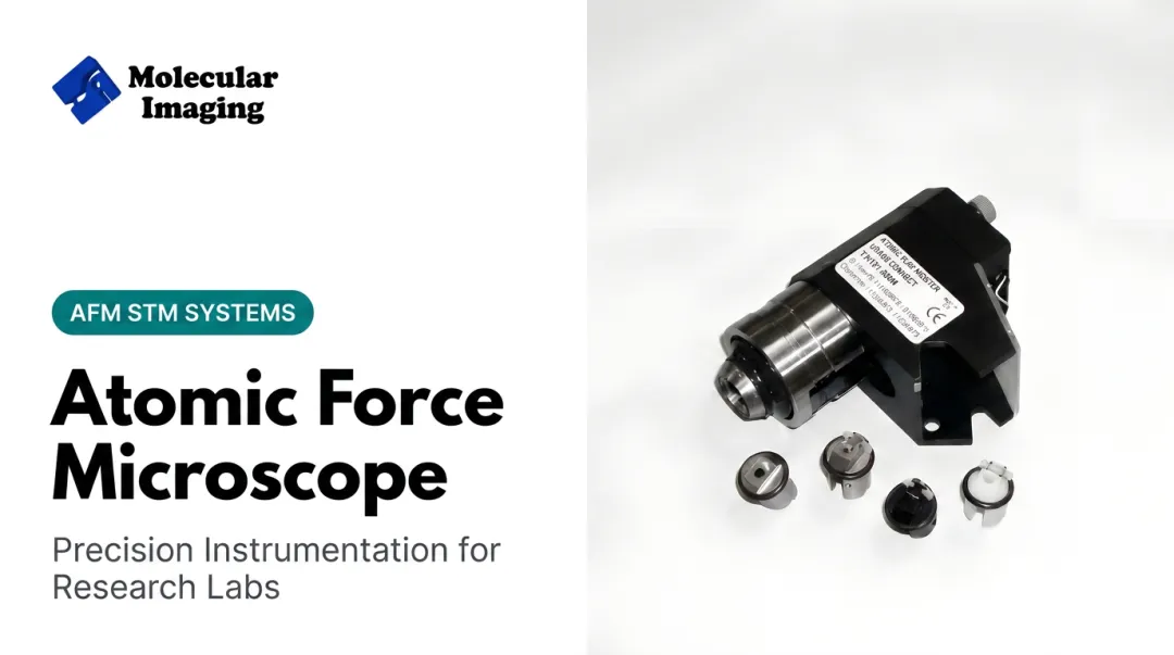
Molecular Imaging's 5500, 5100, and 5420 series platforms are built around this modularity. They support AFM, STM, and nanomechanical characterization on a single interchangeable-nose-cone scanner, rather than requiring a separate box for each technique.

Add an Environmental Isolation Chamber or a temperature-controlled stage, and the same system can move from CVD graphene at room temperature to a reactive-gas battery study without a hardware swap.
For labs already running Agilent-era AFM/STM systems, ZoomAFM provides remote diagnostics, calibration, and repair support, plus on-site service when needed. Coverage includes the 5500, 4500, and other legacy Agilent AFM/STM models.
Frequently Asked Questions
What is atomic force microscopy and how does it work?
A sharp tip on a flexible cantilever scans the sample surface while a laser and photodetector track cantilever deflection. A feedback loop maintains constant force or oscillation, generating a 3D topography map.
Why is AFM preferred over electron microscopy for graphene characterization?
AFM directly measures true vertical thickness through step-height detection, something electron microscopy struggles with. It also operates in air or liquid, avoiding the vacuum requirements that can limit sample handling.
Can AFM measure the number of layers in graphene?
Yes. Height profiling across a flake edge, combined with histogram analysis of step heights, distinguishes mono-, bi-, and multilayer regions based on apparent thickness increments.
What AFM modes are used to study 2D material properties beyond topography?
Kelvin probe force microscopy (KPFM), piezoresponse force microscopy (PFM), lateral force microscopy, and conductive AFM all add electrical, mechanical, or frictional data alongside shape.
Does AFM require special environmental conditions for 2D material samples?
Materials like black phosphorus and MXenes degrade quickly in ambient air. Glovebox-compatible AFM systems with humidity and oxygen control are often necessary to get reliable, repeatable measurements.
How does AFM help in graphene device fabrication?
A biased AFM tip can locally oxidize or cut graphene through local anodic oxidation, enabling mask-free, site-specific patterning for prototype devices and junctions.