But picking between these two scanning probe techniques trips up a lot of labs. Sample conductivity, budget, required resolution, and imaging environment all factor into the decision, and getting it wrong means wasted time or an instrument that can't handle your actual samples.
This guide breaks down how AFM and STM work, where they differ, and how to decide (or combine both) for your specific research goals.
Key Takeaways
- AFM measures probe–surface force and works on nearly any sample, including insulators and biological materials
- STM measures tunneling current for true atomic-scale resolution, but needs a conductive sample
- AFM and STM complement each other; many labs run both rather than choosing only one
- Pick the method by sample conductivity, required resolution, and imaging environment
What is Atomic Force Microscopy (AFM)?
AFM builds surface maps by physically sensing forces between a tiny probe and a sample. It works on conductors, insulators, polymers, and wet biological specimens alike, which is a big reason it has become the more widely deployed of the two techniques.
How AFM Works
A cantilever with a sharp tip, often just a few nanometers at the apex, scans across the sample surface. As the tip encounters topography changes, tip-sample forces bend the cantilever according to Hooke's law.
A laser reflects off the cantilever's back onto a position-sensitive photodiode. Even tiny deflections shift where that laser spot lands (PMC, 2023).
That deflection signal feeds a feedback loop. The system adjusts the z-axis height (or, in tapping mode, the oscillation amplitude) to keep the interaction constant. Track that adjustment across the whole scan area, and you get a detailed 3D topographic map.
AFM Imaging Modes
Different samples call for different levels of tip-sample contact:
| Mode | How it works | Best for |
|---|---|---|
| Contact | Tip stays in continuous physical contact; feedback holds a preset load force | Hard, well-adhered surfaces and faster scans |
| Tapping/intermittent contact | Cantilever oscillates near resonance, touching the surface only briefly each cycle | Soft or fragile samples that continuous contact would damage |
| Non-contact | Tip oscillates above the surface in the attractive-force regime, never touching | Delicate biological or polymer samples needing minimal force |
Contact mode moves fast but can drag, scratch, or displace loosely bound material. Tapping and non-contact modes trade some speed for a gentler touch, which matters once you're imaging something alive.

Common AFM Applications
AFM's flexibility across sample types shows up in how broadly it's used:
- Polymer analysis — mapping surface physicochemical properties and structural dynamics at high resolution
- Battery research — operando KPFM tracking contact-potential changes in working Li-ion cells during charge/discharge (Nature Communications Chemistry, 2019)
- 2D materials — atomic resolution of graphene and graphite has been demonstrated in ambient air, not just vacuum
- Thin film characterization — tapping-mode AFM has resolved submolecular lattice structure in spin-coated polymer films
Biological imaging is where AFM really separates itself from STM. Because it doesn't require conductivity, AFM can image live cells and biomolecules directly in liquid, under near-physiological conditions. Molecular Imaging's BioAFM systems are built specifically for this kind of work, using low-force imaging modes designed to preserve delicate biological structures during extended sessions.
What is Scanning Tunneling Microscopy (STM)?
STM was the original scanning probe technique, and it remains the gold standard when true atomic resolution on a conductive surface is the goal.
How STM Works
STM brings an extremely sharp, conductive tip within less than a nanometer of a conductive sample. Apply a small bias voltage, and electrons tunnel across that gap through quantum mechanics rather than physical contact. Because this tunneling current changes almost exponentially with tip-sample distance, even tiny height variations produce a strong, measurable signal (NIST, 2025).
A feedback loop adjusts either tip height or bias voltage to hold that current steady. Recording those adjustments across the scan builds a map of physical topography and the sample's electronic density of states. AFM's force-based approach can't fully replicate that electronic detail.
STM Modes: Constant Current vs. Constant Height
STM operates in one of two feedback configurations, and the choice depends heavily on how flat your sample is:
- Constant current mode: The tip height continuously adjusts to hold tunneling current steady. This handles uneven or stepped surfaces well, though scanning is slower since the feedback loop has to keep working.
- Constant height mode: The tip stays at a fixed height while current fluctuates with topography. Scans run much faster, but a step or defect can cause a tip crash, so this mode demands an atomically flat sample.

STM Applications and Limitations
STM's atomic-scale sensitivity has made it indispensable in several fields:
- Semiconductor research: resolving structural, electronic, and chemical properties of clean surface reconstructions
- Molecular electronics: bridging single molecules between tip and substrate to measure conductance through individual junctions
- Electrochemistry: imaging electrified interfaces under real reaction conditions for atomic-scale catalyst studies
The catch is unavoidable: STM only works on samples with a conductive tunneling path. Bulk insulators, most polymers, and untreated biological specimens simply won't produce a tunneling current. This limitation is precisely what pushed researchers toward developing an alternative technique in the first place.
AFM vs STM: Key Differences
Both instruments fall under the scanning probe microscopy umbrella, but they rest on entirely different physical principles.
| Criterion | AFM | STM |
|---|---|---|
| Measured interaction | Mechanical force via cantilever deflection | Quantum tunneling current |
| Sample conductivity | Works on conductors and non-conductors | Requires a conductive sample |
| Resolution | Nanometer-scale typically; atomic resolution possible on suitable samples | Atomic and electronic resolution as standard |
| Environment | Air, liquid, or vacuum | Ambient air/gas, ultra-high vacuum, or electrochemical liquid interfaces |
| Damage risk | Contact mode can drag or scratch; tapping/non-contact reduce this | No mechanical contact, though constant-height scans risk tip crashes on steps |
Sample prep also differs in practice. AFM tolerates rough, uneven, or wet samples reasonably well. STM demands a genuinely clean, conductive surface, and for the highest resolution work, often a controlled vacuum environment too.
How AFM Emerged From STM’s Limits
Those sample and conductivity limits are exactly why a second instrument had to be invented. STM came first. Gerd Binnig and Heinrich Rohrer built the original instrument at IBM Zurich in 1981, an achievement that earned them half of the 1986 Nobel Prize in Physics (IBM, n.d.). But STM's conductivity requirement left insulating and biological surfaces off-limits.
That gap led Binnig, Calvin Quate, and Christoph Gerber to publish their design for the atomic force microscope in Physical Review Letters in March 1986, explicitly framing it as a way to study insulator surfaces at atomic scale (Physical Review Letters, 1986). AFM extended probe microscopy to insulators and biological surfaces STM could not image, while STM remained the standard for atomic-scale electronic structure on conductive samples.
Choosing the Right Technique for Your Research
Start with one question: is your sample conductive?
If yes, and you need atomic or electronic-level detail, STM is usually the better fit. It excels at surface reconstructions, molecular junctions, and catalytic interfaces where electronic structure matters as much as topography.
If no — or if you're working with polymers, biological specimens, or anything with unknown/variable conductivity — AFM is the practical choice. It's also the only realistic option when live cells or biomolecules need imaging in their native liquid state.
Environmental needs matter just as much:
- Liquid or ambient imaging (biological studies, electrochemistry): AFM handles this natively
- Ultra-clean, controlled surface studies: STM in UHV delivers the sharpest atomic detail
- Variable temperature experiments: Temperature-controlled stages extend either technique's range for phase transition or thermal studies
Conductivity and environment make the first cut. Beyond that, many advanced applications don't force a binary choice at all. Electrochemistry and molecular electronics research routinely benefit from combined AFM/STM capability. Imaging the same sample with both force-based and tunneling-based contrast maps structure and electronic behavior in a single workflow.
Molecular Imaging's AFM/STM Solutions for Your Research
Molecular Imaging builds on original technology developed before Keysight Technologies exited the AFM market in 2018. A team of former employees, led by Dr. Song Xu, revived the line to close that gap. The result is a modular product line covering nanotechnology, materials science, and life sciences research.
Labs choosing between AFM and STM—or that need both—can match the decision to these systems:
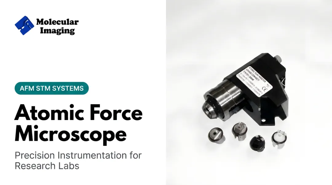
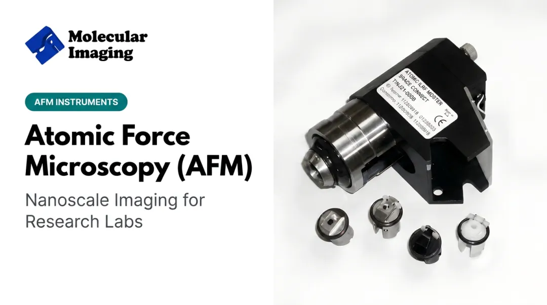
- 5420 PicoAFM: quick-swap nose cones switch between AFM, STM, and force measurement on one instrument
- 5500 PicoPlus AFM+STM: integrated AFM, STM, CSAFM, tapping, KPFM, EFM, and MFM, plus in-situ electrochemistry for battery and corrosion work
- 5500 ILM PicoPlus BioAFM: designed for liquid and live-cell imaging; MAC Mode avoids the spurious resonances that affect standard tapping in fluid
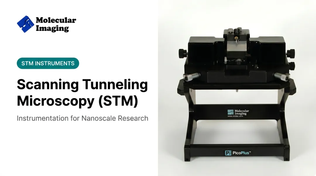
- 4500 PicoSTM: dedicated STM for atomic-resolution work on conductive surfaces

Environmental control accessories extend what you can run on the bench:
- Temperature-controlled stages from -30°C to 250°C for phase-transition studies
- Environmental isolation chambers that regulate humidity, temperature, and gas composition for reactive materials or battery research
For labs with existing AFM or STM systems already on the bench, ZoomAFM provides diagnostics, preventive maintenance, calibration, and both remote and on-site repair support using platform-matched replacement parts. The Molecular Imaging web store also stocks cantilevers, STM tips, and calibration samples for ongoing operation.
Not sure which configuration fits your research? Call 1-888-644-0389 for help matching a system to your work.
Frequently Asked Questions
Are STM and AFM the same?
No. Both are scanning probe microscopy techniques used for surface imaging, but they rely on different physics — tunneling current versus mechanical force — and have different sample requirements.
Which microscope came first, the AFM or the STM?
STM came first, invented in 1981 by Binnig and Rohrer at IBM. AFM followed in 1986 specifically to image insulating surfaces that STM couldn't handle.
Can AFM and STM be used on the same sample?
Yes, if the sample is conductive. Platforms such as the 5500 PicoPlus AFM+STM let researchers switch between modes on one system and collect complementary data from the same sample.
Does AFM require a vacuum environment?
No. AFM operates in air, liquid, or vacuum. STM, by contrast, typically performs best in ultra-high vacuum when atomic resolution is the goal.
What resolution can AFM and STM achieve?
STM resolves individual atoms and electronic states on conductive surfaces as standard. AFM typically delivers nanometer-scale resolution, with atomic resolution achievable under favorable sample and mode conditions.
Which technique is better for biological samples?
AFM. It images soft, non-conductive samples directly in liquid, preserving live cells and biomolecules under near-physiological conditions without the conductivity demands—and related damage risk—that STM would impose.