Introduction
Every atomic force microscope image lives or dies by one tiny component: the probe. It's the cantilever-and-tip assembly that touches (or nearly touches) your sample and turns nanoscale forces into topography, mechanical data, and electrical signals.
Get the probe wrong, and even a strong AFM system returns blurry, artifact-riddled results. Doubled features, unexplained streaking, or resolution that drops mid-session often trace back to the wrong spring constant, an incompatible coating, or a tip worn past useful sharpness—not the instrument.
The market reflects how central these tiny components have become. The global atomic force microscopy market, covering systems and probes together, is projected to grow from $541.8 million in 2025 to $762.2 million by 2030, according to MarketsandMarkets.
This guide walks through what you need to choose and maintain probes with confidence:
- Probe anatomy and how tip and cantilever shape the data
- Imaging modes and when each probe type fits
- Materials, coatings, and application-specific selection
- Practical care so tips stay sharp longer
Key Takeaways
- Tip sharpness, not the microscope itself, sets your lateral resolution limit
- Spring constant and resonance frequency determine which imaging mode a probe suits
- Coatings extend the probe to C-AFM, MFM, and KPFM
- Matching probe to sample and environment prevents wasted scans and damaged tips
- Replace probes based on performance signs, not a fixed calendar schedule
What Is an AFM Probe?
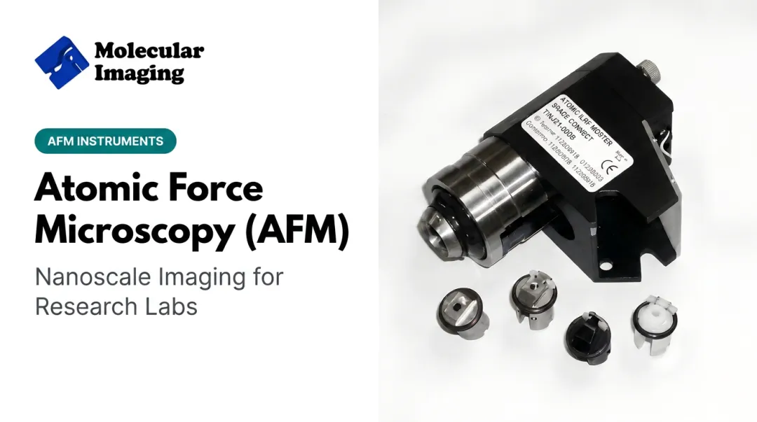
An AFM probe is a microfabricated assembly built from three parts: a flexible cantilever, a sharp tip at its free end, and a support chip that lets you handle and mount the whole thing into the microscope head. Together, they "feel" nanoscale forces—van der Waals attraction, electrostatic pull, mechanical repulsion—that a microscope's optics could never directly see.
Tip Geometry Determines Resolution
The tip apex—not the AFM's optics or electronics—sets lateral image resolution. Standard silicon tips run a typical radius under 8 nanometers, with most manufacturers guaranteeing under 12 nanometers. Supersharp variants push that down to roughly 2 nanometers typical, guaranteed at 5 nanometers or better in over 80% of units, according to NanoWorld's product specifications.
That difference matters when you're trying to resolve individual protein domains or fine grain boundaries in a thin film. A blunter tip simply can't separate features sitting closer together than its own radius.
Spring Constant and Resonance Frequency
Two mechanical properties define what a cantilever can do:
- Spring constant (N/m): how much force is needed to deflect the cantilever. Soft cantilevers (roughly 0.07-0.4 N/m) suit delicate contact-mode work; stiffer ones (20-80 N/m or higher) handle tapping and non-contact imaging on harder samples.
- Resonance frequency (kHz to MHz): how fast the cantilever vibrates when driven near its natural frequency. Standard tapping probes typically resonate between 250-390 kHz, while specialized high-speed probes reach into the megahertz range.
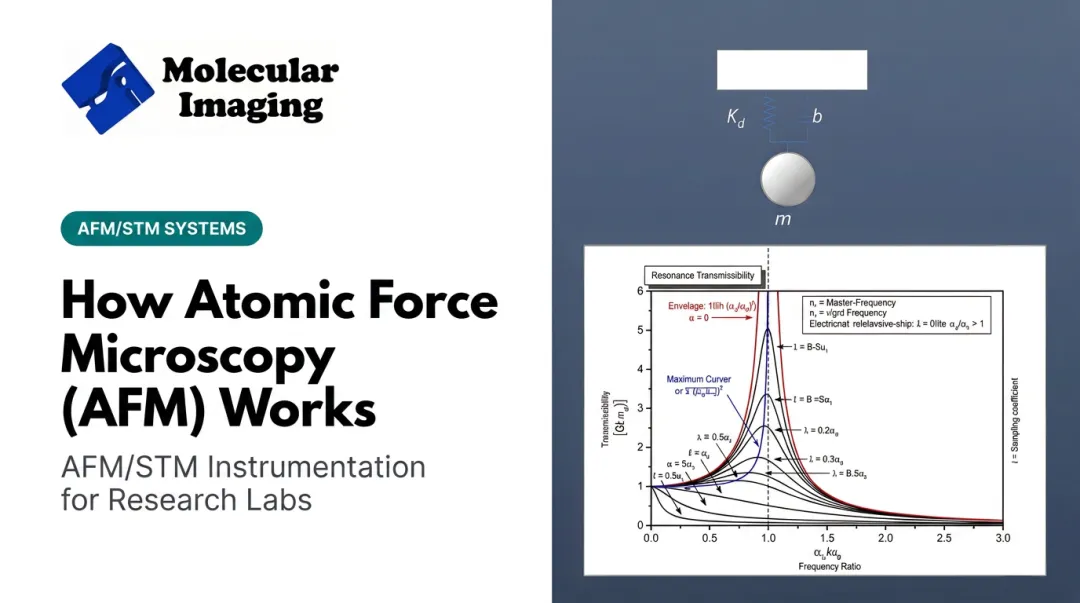
More than any other specs, these two numbers dictate which imaging mode and sample type a probe is built for.
The Support Chip
The support chip, typically around 1.6mm by 3.4mm, is the part your tweezers actually touch. It holds the cantilever rigid and lets the probe seat correctly into the AFM head's holder without you ever handling the fragile tip directly.
Probes Are Consumables, Not Permanent Fixtures
Every probe wears out. Repeated scanning, occasional tip-sample crashes, and surface contamination all shorten a probe's useful life. Exact cost and lifespan vary by material, coating, and how hard you push the probe. There's no single number that applies across every lab. Diamond-coated and conductive-diamond variants are built for extended durability, with some diamond probes demonstrated to hold stable electrical contact through 24-plus hours of continuous use. Budget for regular replacement as a standard line item, not an occasional surprise.

How AFM Probes Work: Core Imaging Modes
Three base imaging modes account for most AFM work. Each demands different cantilever mechanics, and picking the wrong one is the fastest way to damage a sample or a tip.
Contact Mode
The tip stays in continuous contact with the sample, dragging across the surface while feedback electronics hold cantilever deflection constant. This requires soft cantilevers, generally with spring constants at or below 1 N/m, so the tip doesn't gouge the surface or itself. Contact mode delivers fast, stable imaging on sturdier samples but generates lateral shear forces that can smear soft or loosely bound structures.
Tapping (Intermittent Contact) Mode
Here the cantilever oscillates near its resonance frequency, letting the tip touch down only briefly on each cycle. As the tip approaches the surface, interaction forces damp the oscillation amplitude, and that amplitude change becomes the feedback signal. Because contact is fleeting, lateral forces drop substantially, making tapping mode the default choice for polymers, thin films, and many biological samples that can't tolerate constant tip drag.
Non-Contact Mode
Non-contact mode keeps the tip oscillating at small amplitude entirely within the attractive force regime, never touching the surface. Frequency-modulation feedback tracks tiny shifts in resonance caused by long-range forces, delivering the highest sensitivity and, under vacuum, near-atomic resolution. It's demanding to set up and rarely used outside specialized vacuum systems, but no other mode reaches the same force sensitivity.
Beyond Topography: Mode-Driven Techniques
These three base modes also underpin specialized techniques that reuse the same cantilever hardware differently:
- Conductive AFM (C-AFM) — maps local current flow through the sample
- Magnetic Force Microscopy (MFM) — resolves magnetic domain structure
- Kelvin Probe Force Microscopy (KPFM) — maps surface potential and work function
The same cantilever platform supports these extra channels once you match tip coating and electronics to the measurement.
The Frontier: Ultrafast, Sub-Picometer Probes
Probe design keeps advancing. A research team led by L. Schwab demonstrated a silicon optomechanical AFM probe with a mechanical resonance above 130 MHz and a displacement noise floor below 3 × 10⁻¹⁶ m/√Hz, published in Microsystems & Nanoengineering in 2022. That's several hundred times faster than a standard tapping probe's resonance, opening the door to force sensing at speeds previously unreachable. Still a research-grade demonstration rather than a catalog part, it sets the performance bar high-speed AFM probe design is chasing next.

Types of AFM Probes: Materials & Coatings
The base material and coating of a probe determine what it can measure, not just how it images topography.
Silicon: The Workhorse
Monolithic silicon probes dominate general-purpose AFM work. Their high stiffness-to-mass ratio suits tapping and non-contact modes, where the cantilever must vibrate cleanly at hundreds of kilohertz without excessive damping. Molecular Imaging's ContSi-10 and NCH-30-10 cantilevers cover contact and high-frequency tapping and are compatible with all major brand AFM systems for most standard air-environment imaging.
Silicon Nitride: Softer and More Forgiving
Silicon nitride cantilevers flex more easily, with lower spring constants that make them the default choice for contact mode and for biological or liquid-environment imaging. Lower interaction forces mean less risk of damaging a cell membrane or denaturing a protein mid-scan. Products like the S3N4-10 and liquid-optimized Si3N4-L-10 are built for biological and polymer samples in aqueous media.
Conductive Coatings for Electrical Measurements
Gold, platinum, and doped diamond coatings turn a standard probe into an electrical sensor for C-AFM, KPFM, and EFM. That matters in molecular electronics and battery research, where topography and conductivity need to come from the same scan. One caveat: some cantilevers carry gold only on the reflective backside to boost laser signal, not on the tip. Confirm which surface is coated before assuming the probe is tip-conductive.
Magnetic Coatings for Domain Mapping
Hard magnetic coatings enable Magnetic Force Microscopy, letting researchers visualize magnetic domain structures on data storage media, spintronic devices, and magnetic thin films. Molecular Imaging's MFM-10 cantilever serves this role across the 5500 and related platforms.
Specialty Tips
- Diamond-coated tips (including Diamond-10): wear-resistant for nanoindentation and scanning probe lithography on hard materials
- Supersharp silicon tips: radii near 2 nm for maximum lateral resolution on flat, hard samples
- Etched Pt-Ir tips (STM Etched and Insulated): atomic-resolution STM imaging and electrochemical work Researchers can source this full range—cantilevers, calibration samples, substrates, and STM tips—through Molecular Imaging's web store, which supports Agilent-based AFM/STM systems used across nanotechnology, life science, and materials labs.

Choosing the Right AFM Probe for Your Application
Choosing a probe comes down to three questions: how stiff is your sample, what environment are you imaging in, and what property are you actually trying to measure?
Match Mechanics to Sample Stiffness
- Soft biological samples (cells, proteins, DNA) need low spring constants, generally under 0.5 N/m, to avoid deformation
- Hard materials (ceramics, metals, semiconductors) benefit from stiffer, higher-frequency probes that resist twisting and give sharper feedback
- When in doubt, start softer. A probe too stiff for the sample causes damage that can't be undone; one too soft just underperforms
Factor In the Imaging Environment
Air, liquid, and vacuum each favor different probes:
- Air: most standard silicon probes work well
- Liquid: silicon nitride or gold-coated probes for reduced resonance shift in fluid; MAC Mode probes with paramagnetic coatings for gentle oscillation control
- Vacuum: non-contact frequency-modulation setups with high-Q silicon cantilevers
Align Probe Choice with Research Goal
Simple topography mapping rarely needs anything exotic. A standard tapping probe usually does the job. But once you need more than a height map, coating choice becomes the deciding factor:
| Research Goal | Probe Type Needed |
|---|---|
| Topography only | Standard silicon tapping probe |
| Electrical conductivity mapping | Pt, PtIr, or doped diamond conductive coating |
| Magnetic domain imaging | Hard magnetic coating (such as MFM-10) |
| Mechanical property/hardness testing | Diamond-coated indentation probe |
| Biological/liquid imaging | Silicon nitride or MAC Mode probe |
Getting this match right the first time saves both the probe and the sample, and it's usually cheaper than re-running a failed scan session.
AFM Probe Applications Across Research Fields
Life Sciences and Bio-AFM
Soft silicon nitride probes make it possible to image proteins, DNA, and cell membranes directly in fluid, without fixing or staining the sample first.
In one widely cited study, researchers used tapping-mode silicon probes (around 50 N/m, 170 kHz) to image MutS-DNA mismatch repair complexes. They distinguished bent and unbent protein-DNA populations at the single-molecule level (Journal of Biological Chemistry).
Typical bio-AFM needs include:
- Soft cantilevers for proteins, DNA, and membranes in fluid
- Low-force imaging without fixation or staining
- Stable drive in liquid (for example, MAC Mode)
Molecular Imaging's Si-L-10 and Si3N4-L-10 liquid cantilevers, paired with MAC Mode's paramagnetic drive, support this kind of gentle, in-fluid biomolecular work.
Materials Science and Nanotechnology
Standard silicon tapping-mode probes remain the backbone of thin-film, polymer, and nanostructure characterization.
Phase imaging with these probes can separate chemically different polymer domains in the same film. Published work has mapped polystyrene/polybutadiene blend heterogeneity at the 250-nanometer scale—contrast that standard optical microscopy cannot show.
Common materials applications include:
- Thin-film and polymer domain mapping
- Nanostructure metrology on hard samples
- Phase contrast beyond optical limits
Tapping-mode silicon cantilevers such as the NCH-30-10 handle this work routinely.
Electrochemistry and Molecular Electronics
Conductive probes enable in-situ electrochemical AFM (EC-AFM), where topography and electrical transport get measured simultaneously as a reaction unfolds in real time. Published research has used this approach to visualize solid-electrolyte interphase (SEI) nucleation and growth on lithium-ion battery electrodes, finding that SEI layers on some carbon anodes formed roughly twice as thick, and mechanically stronger, than on others.
The 5500 and 5420 systems support in-situ electrochemical AFM with liquid cells rated for acids, bases, and organic solvents. Conductive AFM enables conductivity mapping on TiW films, SiGe heterostructures, and related molecular electronics samples.

Across life science, materials, and electrochemistry work, matching probe stiffness, coating, and environment to the sample is what turns AFM from a general imager into a field-specific measurement tool.
AFM Probe Care, Wear, and When to Seek Professional Service
What Wears Out a Probe
Three culprits account for most probe degradation:
- Contamination: airborne particles, sample residue, or oxide buildup coat the tip and blur measurements
- Mechanical wear: repeated scanning gradually rounds off even a sharp tip, widening its effective radius
- Tip-sample crashes: a single hard impact, often from an incorrect approach setting, can blunt or snap a tip instantly
Basic Probe Care
A few habits extend tip life between swaps:
- Handle the chip by its edges—never touch the cantilever or tip
- Store unused probes in their original gel box, tip-side protected
- Keep the scan area free of dust, aerosols, and unnecessary sample debris
- Use a controlled approach; rushed engage settings cause most crash damage
Recognizing a Failing Probe
Watch for these warning signs during a scan:
- Image doubling or "ghost" features that shouldn't be there
- Streaking artifacts running across scan lines
- Gradual resolution loss mid-session on samples that imaged cleanly earlier
Any of these usually means it's time to swap the probe before troubleshooting anything else.
When Probe Replacement Isn't Enough
If a fresh probe doesn't fix the problem, the issue likely sits deeper in the instrument: thermal drift, vibration isolation, feedback loop instability, or a misaligned laser-photodetector path. At that point, professional evaluation makes more sense than continuing to swap consumables.
Molecular Imaging's ZoomAFM service diagnoses and repairs legacy Agilent 5500 and 4500 AFM/STM systems, including precision calibration and custom replacement parts. Labs on older platforms can restore performance without replacing the whole instrument.
Frequently Asked Questions
What does an atomic force microscope measure?
AFM measures surface topography by tracking cantilever deflection. Depending on the probe type, it can also map forces such as van der Waals, electrostatic, capillary, and magnetic interactions, plus mechanical or electrical properties.
What is the difference between scanning probe microscopy and atomic force microscopy?
Scanning probe microscopy (SPM) is the umbrella category that includes AFM, STM, and related techniques. AFM specifically detects force-induced cantilever deflection, while STM measures tunneling current between a conductive tip and sample.
How often should AFM probes be replaced?
There is no fixed schedule. Replace a probe when you see image doubling, streaking, or declining resolution, or when it's visibly contaminated or has suffered a tip-sample crash.
Can the same AFM probe be used for multiple imaging modes?
Generally, no. Probes are optimized for a specific spring constant, resonance frequency, and coating combination tied to one mode and sample type, so switching modes usually means switching probes too.
What is the typical tip radius of an AFM probe?
Standard silicon tips run under 8 nanometers, typically guaranteed below 12 nanometers. Supersharp tips reach roughly 2 nanometers, useful for resolving fine features on flat, hard samples.
Where can researchers source replacement AFM probes and accessories?
Specialized suppliers carry the full range of cantilevers, calibration samples, and substrates. Molecular Imaging's web store offers probes, calibration gratings, and mica/gold substrates compatible with all major brand AFM systems - browse the catalog or contact the team for mode-specific recommendations.