Researchers running STM experiments know the frustration: a tip that imaged beautifully yesterday suddenly produces streaky, doubled, or unstable results today. Contamination, blunting, and oxidation are constant threats to reproducible data.
This article breaks down the tip materials that matter, how to prepare them, common artifacts to watch for, and how to match material choice to your specific research application.
Key Takeaways
- Atomic-scale apex geometry, not the visible wire shape, determines your achievable resolution
- Tungsten and platinum-iridium (Pt/Ir) dominate STM tip material choices, each with distinct trade-offs
- Consistent etching, cutting, and in-situ conditioning reduce artifacts and variability
- Match tip material to your environment: UHV, ambient air, or electrochemical conditions
Why Tip Material Matters in STM
STM works because of quantum tunneling. Electrons cross the vacuum gap between tip and sample even though classically they shouldn't be able to. The tunneling current depends exponentially on tip-sample distance. Molecular STM research describes that decay with a typical barrier height around 3–4 eV.
That exponential relationship means tiny changes at the atomic scale produce huge changes in signal. A single atom protruding from the tip apex carries most of the tunneling current.
Tip material shapes three things:
- Conductivity — affects signal stability and noise
- Chemical stability — determines how long a tip stays clean and usable
- Durability — governs how many scans you get before re-preparation
There's also an electronic dimension separate from topography. Current is a convolution of both tip and sample density of states, according to Harvard's STM research notes. The same sample can look different under two tips made of different materials because of that electronic contribution, not physical height differences.
Resolution Depends on the Apex, Not the Wire
A commonly cited academic benchmark places STM resolution at roughly 0.1 nm lateral and 0.01 nm vertical, but this only holds with clean surfaces and sharp, stable tips. Boston College's tip-preparation guidance notes that a good tip apex should have a curvature radius of 50 nm or less. Blunt tips spread the tunneling region across multiple atoms, smearing fine detail.

When Tips Go Wrong
A contaminated or multi-apex tip doesn't just lose resolution. It introduces artifacts:
- Double-tip imaging — duplicated features across the scan
- Streaking — noisy, unstable lines during a scan
- Sudden contrast shifts — often from a picked-up contaminant atom
Common STM Tip Materials Compared
Tungsten (W) Tips
Tungsten remains a workhorse material. It's hard, conducts well, and etches into atomically sharp points relatively easily using standard electrochemical methods.
The catch: tungsten oxidizes fast in ambient air. Bruker's probe documentation recommends discarding tungsten tips after just 1-2 days of air exposure if you need consistent performance. That makes tungsten best suited to UHV environments where in-situ cleaning (annealing, sputtering) keeps the apex oxide-free.
Platinum-Iridium (Pt/Ir) Tips
Pt/Ir tips trade some sharpness potential for chemical resilience. They resist oxidation far better than tungsten, which is why they're the default choice for ambient-air and electrochemical STM work.
Trade-offs to know:
- Softer than tungsten, so mechanical wear happens faster under rough handling
- Harder to etch to the same atomic sharpness as tungsten
- Generally more expensive per tip
Those trade-offs are why Molecular Imaging's web store centers on Pt/Ir tips. The etched PT-IR Tip PT-10 is built for high-resolution atomic imaging; the insulated PT-IR Tip PT-10 supports electrochemical and localized spectroscopy work where tunneling current must stay below roughly 70 pA.
Other and Specialized Materials
A few niche materials serve specific research needs:
- Gold tips: used for tip-enhanced Raman spectroscopy (TERS), not standard STM imaging
- Carbon nanotube-modified tips: SWNT-functionalized gold tips enable chemically selective imaging through hydrogen-bond-mediated tunneling
| Material | Chemical Stability | Etching Ease | Best Environment |
|---|---|---|---|
| Tungsten | Oxidizes quickly in air | Easy, well-established | UHV |
| Pt/Ir | Chemically inert | Harder to sharpen | Ambient, electrochemical |
| Gold | Application-specific | Specialized fabrication | TERS, nanofabrication |
| CNT-modified | Niche, selective | Complex functionalization | Chemically selective molecular imaging |

Tip Preparation and Sharpening Techniques
Electrochemical Etching for Tungsten
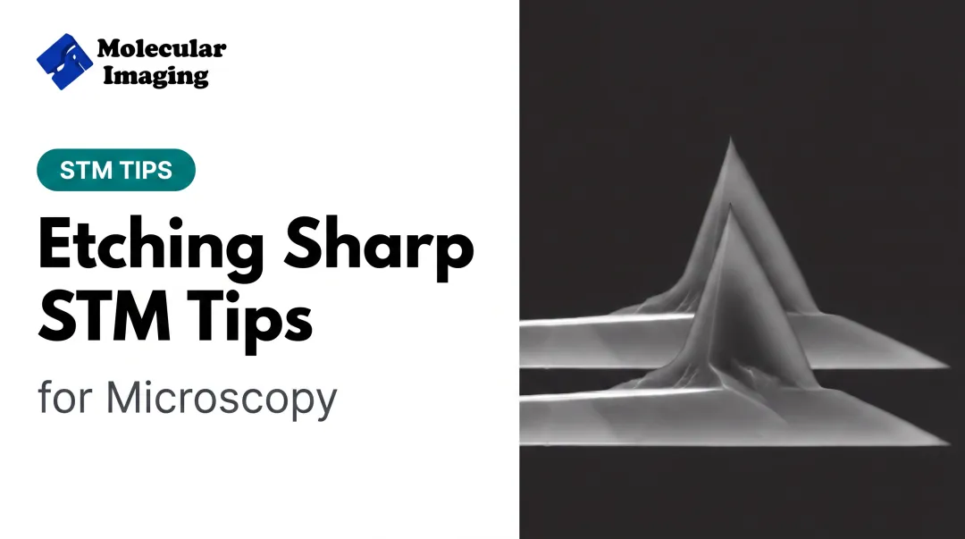
The standard method submerges tungsten wire in an etchant (commonly KOH or NaOH) and applies a DC bias until the wire necks and drops off, leaving a sharp apex behind.
Published protocols show real variation in outcomes:
- Two-step etching reaches curvature radii below 10 nm with roughly 90% success when a fast drop-off circuit stops etching within nanoseconds of break
- One-step etching produces radii below 40 nm with closer to 80% success
Timing control is critical. Continued current flow after the wire snaps blunts the tip immediately.

Mechanical Cutting for Pt/Ir
Since Pt/Ir is harder to etch cleanly, many labs cut it mechanically instead. Bruker's documentation describes cutting 0.25 mm wire at a 45-degree angle while pulling and twisting during the snip: a simple, repeatable alternative to electrochemical etching. Labs that prefer not to cut in-house can also source pre-etched Pt/Ir tips as consumables.
In-Situ Conditioning
Once mounted, tips can be reconditioned without removing them from the instrument:
- Voltage pulsing: a brief high-field pulse can move or eject apex atoms, reshaping a damaged tip
- Field emission: cleans loose contamination from the apex
- Controlled contact: a gentle tip–sample touch can reform the apex when pulsing alone is not enough
Consistent preparation protocols drive imaging quality. Session-to-session variability often traces back to inconsistent etching or cutting technique, not the sample itself.
Tip-Related Artifacts and Troubleshooting
Recognizing the Problem
Double-tip or ghost imaging happens when the apex has two or more conducting points instead of one. Each sample feature gets imaged twice, offset by a fixed vector. Computational correction through crystallographic averaging can sometimes help, but only on periodic samples and with clear limits.
Contamination and oxidation show up differently:
- Increased noise during otherwise stable scans
- Sudden loss of atomic resolution mid-session
- Tip instability requiring frequent bias adjustment
Resolving Tip Artifacts
When artifacts appear, try these in order:
- Apply a voltage pulse to reshape or clean the apex without removing the tip
- Re-etch or re-cut if pulsing doesn't resolve it
- Swap the tip entirely if performance doesn't recover after conditioning

Keeping spare, properly prepared tips on hand saves significant downtime. Molecular Imaging's web store carries both etched and insulated Pt-Ir replacements, and its ZoomAFM support line (1-888-644-0389) can help determine whether the issue is the tip or another part of the system.
Matching Tip Material to Your Research Application
Different research settings call for different trade-offs:
- UHV surface science: Tungsten can reach atomic sharpness here because in-situ annealing and sputtering keep oxide off the apex on clean conductive surfaces
- Electrochemistry and ambient conditions: Pt/Ir's oxidation resistance makes it the practical default. Tufts University's chemistry department notes STM also runs in ambient air and under potential control at solid-liquid interfaces, where material stability is critical
- Molecular electronics: Tip-sample electronic coupling shapes image contrast independent of topography, so pick the material for the electronic contrast you need, not only mechanical sharpness Molecular Imaging's 4500 PicoSTM and 5500 PicoPlus AFM+STM platforms support STM work across these settings. Both offer Pt/Ir tip options and electrochemistry accessories, including liquid cells and environmental isolation chambers, for labs that move between ambient, liquid, and controlled-atmosphere experiments.
Frequently Asked Questions
What is the difference between AFM and STM?
STM measures tunneling current between a conductive tip and a conductive sample, requiring an electrical path. AFM measures physical force through cantilever deflection and works on both conductive and insulating samples.
How sharp does an STM tip need to be?
Effective sharpness comes from a single atom or small cluster at the very apex, not the visible macroscopic point of the wire. A tip can look sharp under a microscope and still image poorly if the true apex isn't atomically defined.
Can STM tips be reused or re-sharpened?
Yes, often. Voltage pulsing can recondition a tip in place, and re-etching or re-cutting can restore a damaged apex. Eventually, though, tips wear out and need full replacement.
Why does my STM tip produce double or ghost images?
This usually means the apex has two or more conducting points instead of one, duplicating each sample feature in the scan. Re-etching or applying a voltage pulse to reshape the apex typically resolves it.
Does tip material affect STM image contrast?
Yes. Tip material contributes its own electronic density of states to the tunneling current, which affects contrast independent of the sample's actual topography. Two different tip materials can make the same feature look different.