The market reflects that demand. MarketsandMarkets projects the global AFM market growing from $541.8 million in 2025 to $762.2 million by 2030, a 7.1% CAGR. North America alone represents roughly a third of that market, driven by semiconductor metrology and university research programs.
Choosing the right AFM manufacturer isn't just about brand recognition. This guide breaks down the companies actually serving US research labs today, what makes each one different, and how to pick the right fit for your work.
TL;DR
- AFM maps surface topography and forces at the nanoscale with a cantilever-mounted tip
- Manufacturer choice drives resolution, modularity, application range, and long-term support
- This guide ranks top AFM companies serving US researchers on capability and service reliability
- Molecular Imaging offers modular AFM/STM systems, environmental accessories, and Agilent-era repair support
What Is Atomic Force Microscopy, and Who Uses It?
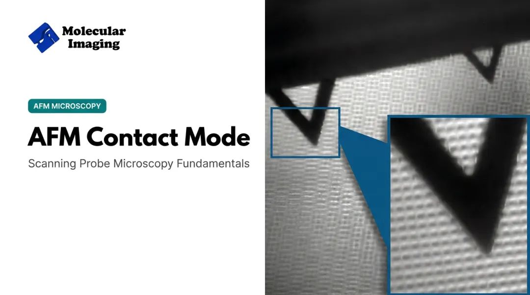
AFM works by dragging (or tapping) a cantilever-mounted tip across a sample surface. A laser tracks the cantilever's motion, and feedback electronics maintain a set measurement condition, generating detailed 3D topographical data at the nanoscale.

Beyond topography, modern AFM systems also measure mechanical, electrical, chemical, and magnetic properties. In the US, that versatility drives demand across several distinct communities:
- University surface-science labs studying fundamental material behavior
- Semiconductor R&D teams measuring roughness, defects, and electrical properties on wafers
- Life-science researchers imaging proteins, cells, and biomolecular interactions in liquid
- Shared instrumentation core facilities supporting dozens of research groups on one platform
Given this range of use cases, no single "best" AFM company exists. The right choice depends on application fit, not just spec sheets. Below, we rank companies on technical capability, modularity, breadth of application support, and, critically, service and repair reliability.
Top Atomic Force Microscope Companies in the US
These companies were evaluated on technical capability, system modularity, application breadth, support quality, and reputation among research institutions.
Molecular Imaging
Molecular Imaging has an unusual origin story. The original company was founded in 1993 by Professor Stuart Lindsay and Dr. Tianwei Jing at Arizona State University, focused on building accessible, modular AFM/STM systems. Agilent Technologies acquired it in 2006, and the brand continued under Agilent (later Keysight Technologies) branding.
When Keysight exited the AFM market in 2018, former employees (led by Dr. Song Xu) reunited to revive the company. Dr. Stuart Lindsay, the original co-founder, now serves as academic advisor.
What makes it different:
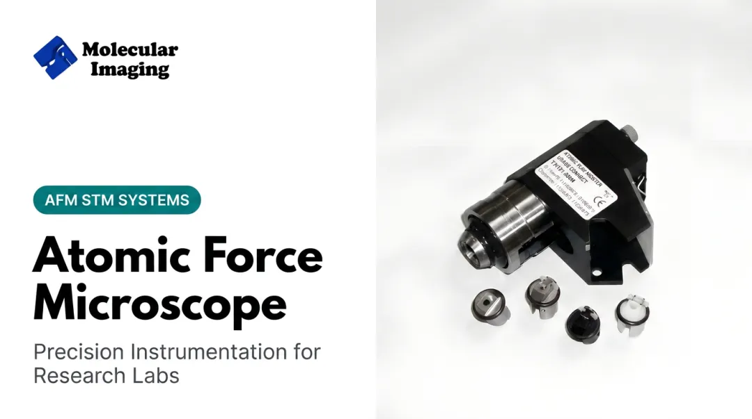
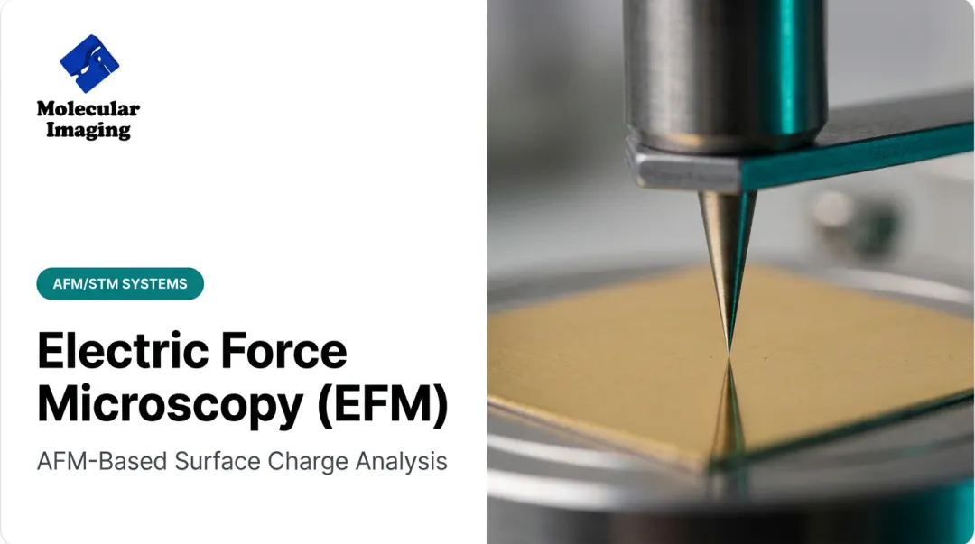
- Modular AFM/STM systems with interchangeable nose cones (AFM, STM, CSAFM, tapping, KPFM/KFM, EFM, MFM)
- Temperature-controlled stages from −30°C to 250°C for phase-transition and thermal studies
- Environmental Isolation Chambers for battery research, polymer analysis, and reactive-gas work
- Strong fit for electrochemistry (in-situ liquid cells) and BioAFM (live-cell and biomolecular imaging)
- ZoomAFM repair and maintenance for existing Agilent-branded AFM/STM owners
Molecular Imaging's product line spans whole-unit platforms like the 4500 PicoSTM, 5420 PicoAFM, 5500 PicoPlus AFM+STM, and 5500 ILM PicoPlus BioAFM, alongside a web store stocking cantilevers, calibration samples, and substrates.
| Category | Details |
|---|---|
| Key Features | Modular AFM/STM design with interchangeable nose cones, BioAFM capability, environmental control accessories |
| Target Users | University labs, materials science R&D, electrochemistry researchers, existing Agilent system owners |
| Support Offering | ZoomAFM Fast Online Service (remote diagnostics, calibration guidance, on-site repair scheduling), web store for parts and consumables |

Bruker Corporation
Bruker is one of the largest names in scientific instrumentation, with an AFM portfolio built for materials science, biology, and nanotechnology at scale. Its systems tend to show up wherever labs need both breadth and depth — from graphene characterization to battery research.
In December 2024, Bruker introduced the Dimension Nexus AFM at the MRS Fall Meeting: a small-footprint, large-sample system running NanoScope 6 software, PeakForce Tapping, and more than 50 AFM modes with a programmable stage for multi-site analysis.
| Category | Details |
|---|---|
| Key Features | High-resolution imaging, BioAFM systems, 50+ operating modes |
| Target Users | Materials science, biotech, semiconductor R&D |
| Notable Innovation | Dimension Nexus AFM (Dec. 2024), with AFM-nDMA for viscoelastic measurements and PeakForce QNM for nanomechanical mapping |

Park Systems Corp.
Park Systems, based in South Korea, built its reputation on non-contact AFM technology and a heavy footprint in semiconductor fabs. Its systems favor automation over manual operation, which helps when you're running high volumes of wafer inspections.
The Park FX40 brings automatic probe exchange (up to eight pre-mounted probes), automatic laser alignment, and SmartScan software for small-sample imaging.
At SEMICON Korea 2025, Park expanded its large-sample lineup with the FX200 and FX300 for 300mm wafer analysis. The FX200 IR and FX300 IR variants combine AFM with FTIR/PiFM for chemical identification below 5nm resolution.
| Category | Details |
|---|---|
| Key Features | True Non-Contact mode, automated probe/laser/sample handling, AI-assisted SmartScan software |
| Target Users | Semiconductor fabs, industrial metrology teams |
| Notable Innovation | FX200/FX300 large-sample lineup, plus FX40 for small-sample high-throughput imaging |

Oxford Instruments (Asylum Research)
Oxford Instruments' Asylum Research division focuses on pairing AFM with complementary analytical techniques, building systems that appeal to labs running multi-modal experiments rather than AFM in isolation.
In May 2025, Oxford launched the Jupiter Discovery AFM, with a noise floor below 25 picometers, an ultra-rigid granite bridge, and scan rates 5-20 times faster than comparable large-sample systems. The platform supports samples up to 210mm in diameter.
A separate release, the Vero VRS1250 (September 2024), adds video-rate imaging using Quadrature Phase Differential Interferometry.
| Category | Details |
|---|---|
| Key Features | Multi-technique integration, sub-25pm noise floor, motorized laser alignment |
| Target Users | Academic labs, materials researchers needing high-sensitivity systems |
| Notable Innovation | Jupiter Discovery AFM (May 2025) and Vero VRS1250 video-rate imaging (Sept. 2024) |
Nanosurf AG
Nanosurf, based in Switzerland, makes its name with compact, approachable AFM systems. That makes them a good fit for teaching labs and cleanroom facilities that don't want a steep learning curve on every measurement.
The DriveAFM platform features WaveMode, an off-resonance imaging technique that turns the cantilever into a dual-function sensor and actuator using CleanDrive photothermal excitation. This approach suits both biological samples and advanced materials.
| Category | Details |
|---|---|
| Key Features | Compact footprint, WaveMode off-resonance imaging, CleanDrive photothermal excitation |
| Target Users | Educational institutions, semiconductor cleanroom facilities |
| Notable Innovation | DriveAFM with WaveMode technology |
Hitachi High-Tech Corporation
Hitachi integrates AFM into a broader portfolio of electron and optical measurement tools, appealing to labs that want cross-technique correlation without juggling multiple vendors.
The AFM100 Pro, launched in 2022, added a newly developed high-sensitivity optical head for improved detection at atomic and molecular scales. Hitachi announced in November 2025 that AFM100 Series and AFM5500MII sales will end once current production is exhausted, with a planned cutoff of September 30, 2026.
| Category | Details |
|---|---|
| Key Features | Software-integrated AFM, one-click autopilot measurement, correlative AFM marking |
| Target Users | Semiconductor and materials science researchers |
| Notable Innovation | AFM100 Pro high-sensitivity optical head (2022); availability window closing in 2026 |
How We Chose the Best AFM Companies
Buyers often default to brand recognition alone, assuming the biggest name automatically fits their application. That's a mistake. A system built for high-throughput semiconductor metrology is not the right tool for a bio-AFM lab imaging live cells in liquid.
We weighed five factors instead:
- Technical capability: resolution, scan range, and available imaging modes
- Modularity and flexibility: whether the system can adapt as research needs change
- Application breadth: strength in one niche versus coverage across multiple disciplines
- Support and repair availability: parts, service, and repair access years after purchase
- Reputation among research institutions: trust and adoption in academic and industrial labs
Service availability deserves more attention than it usually gets. AFM systems are long-term investments, often running for a decade or more. When a manufacturer exits the market or discontinues a line, as Hitachi did with the AFM100 Series, labs are left scrambling for parts and repairs.
Conclusion
The "best" AFM company depends entirely on what you're measuring, how your lab operates, and what happens after the sale. Application fit and service reliability matter more than brand name alone.
Before purchasing, evaluate:
- Scalability: will this system handle your research five years from now?
- Environmental control needs: do you need temperature, humidity, or gas-controlled imaging?
- Total cost of ownership: factor in consumables, calibration samples, and eventual repairs, not just the sticker price
If you already own an aging Agilent-branded AFM or STM system, replacement isn't your only option. Molecular Imaging's ZoomAFM service offers diagnostics, calibration, and repair support built specifically for these legacy platforms.
Its modular AFM/STM systems also remain a strong option for labs working in electrochemistry, materials science, and BioAFM applications.
Frequently Asked Questions
Who are the top microscope manufacturers?
Leading AFM manufacturers serving US labs include Bruker, Park Systems, Oxford Instruments (Asylum Research), Hitachi High-Tech, Nanosurf, and Molecular Imaging. Each targets slightly different applications, from semiconductor metrology to bio-AFM research.
What is an AFM microscope?
An atomic force microscope is a scanning-probe instrument that uses a cantilever-mounted tip to measure surface topography and forces at the nanoscale. It generates detailed 3D data on mechanical, electrical, chemical, and magnetic properties.
Who invented the atomic force microscope?
Gerd Binnig, Calvin Quate, and Christoph Gerber invented the AFM, publishing their work in Physical Review Letters in 1986. The instrument built on scanning tunneling microscopy principles developed earlier by Binnig and Heinrich Rohrer.
How much does an AFM system typically cost?
Pricing varies widely based on modularity, resolution requirements, automation level, and accessories like environmental control chambers. Because configurations differ so much between labs, it's best to consult directly with a manufacturer for an accurate quote.
What industries rely most heavily on AFM technology?
Semiconductors, materials science, nanotechnology, and life sciences are the primary industries using AFM. Applications range from wafer defect analysis to imaging proteins and cell membranes in liquid environments.
Can existing AFM/STM systems be repaired instead of replaced?
Yes. Specialized services like Molecular Imaging's ZoomAFM offer repair, calibration, and maintenance for aging Agilent-branded AFM/STM systems, extending instrument life without the cost of full replacement.