The technology isn't slowing down, either. MarketsandMarkets projects the global AFM market to grow from $541.8 million in 2025 to $762.2 million by 2030, a 7.1% CAGR driven by expanding use across university, industrial, and shared-instrumentation facilities.
Despite how common AFM has become, many users operate these instruments daily without a clear picture of what's actually happening between the tip and the sample. This guide breaks down the mechanics step by step, so you understand not just what AFM shows you, but how it gets there.
Key Takeaways
- AFM "feels" surfaces with a sharp tip on a flexible cantilever instead of using light or electrons
- A laser and photodetector track cantilever deflection as the probe scans line by line
- A feedback loop holds force or oscillation constant, converting tip movement into a height map
- Contact, tapping, and non-contact modes suit different sample types, from hard films to living cells
- Materials science, semiconductors, and biological research all rely on AFM where SEM or optical tools fall short
What Is an Atomic Force Microscope?
An atomic force microscope is a type of scanning probe microscope (SPM) that images surface topography by scanning a sharp tip across a sample and measuring the forces between them. Instead of forming an image from reflected light or focused electrons, it builds a picture point by point from mechanical interaction.
This approach exists because conventional optical microscopes hit a hard wall: the diffraction limit of visible light caps resolution around 200 nanometers. Researchers needed a way to see far smaller features.
In 1986, Gerd Binnig, Calvin Quate, and Christoph Gerber introduced the atomic force microscope in Physical Review Letters, combining principles from scanning tunneling microscopy and stylus profilometry to image insulating surfaces at atomic scale.
Despite the name, AFM uses no lenses, no electron beams, and no nuclear forces. It also differs from its closest relatives:
- Scanning tunneling microscopy (STM) measures tunneling current between a conductive tip and sample, limiting it to conductive materials
- Scanning electron microscopy (SEM) requires a vacuum and often a conductive coating on the sample
- AFM works on virtually any surface, in air, liquid, or vacuum, with no special coating required
That flexibility keeps AFM relevant decades later. It delivers true 3D surface profiles that optical and electron techniques can't match.

AFM operates in several core modes:
- Contact mode — tip stays in constant contact, best for rigid, robust samples
- Tapping (intermittent contact) mode — tip oscillates and briefly touches the surface, gentler on soft or biological samples
- Non-contact mode — tip hovers just above the surface, sensing attractive forces without touching it
Specialized variants extend this further, including Magnetic Force Microscopy (MFM) for mapping magnetic domains, Piezoresponse Force Microscopy (PFM) for ferroelectric materials, and Kelvin Probe Force Microscopy (KPFM) for surface potential.
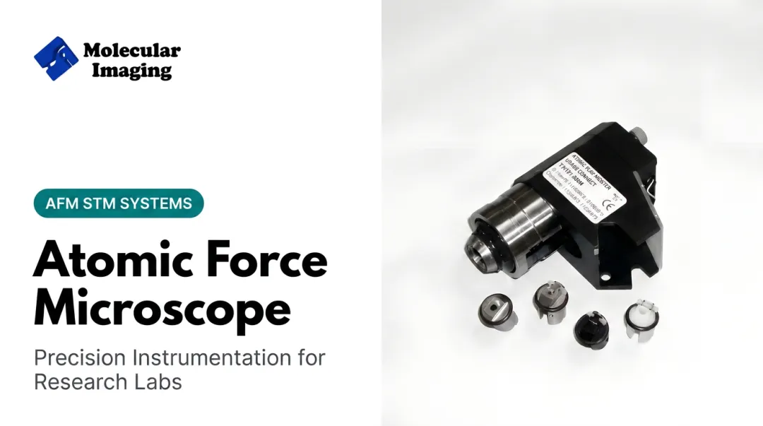
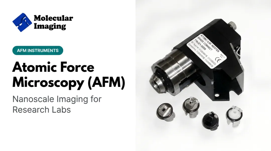
Molecular Imaging builds this flexibility into its hardware. The 5500 PicoPlus AFM+STM and 5420 PicoAFM systems use interchangeable modular nose cones, so one instrument can switch between contact, tapping, non-contact, MFM, and KPFM configurations without separate machines.
How Does an Atomic Force Microscope Work?
AFM follows a defined sequence: position the probe, sense the tip-sample interaction, apply feedback control, and generate a topographic output. Each stage matters, and understanding them helps explain both the images AFM produces and the errors that show up when something goes wrong.
Initiation
Before any imaging happens, the sample gets mounted on a piezoelectric stage, and the cantilever/tip assembly approaches the surface until measurable tip-sample forces appear. This isn't a manual, hand-cranked process anymore. Software-controlled piezoelectric actuators handle the approach automatically, giving repeatable, precise positioning down to fractions of a nanometer.
One detail trips up a lot of new users: tip sharpness and cantilever spring constant have to match the sample. A stiff cantilever meant for hard materials will crush a soft protein sample; a soft cantilever won't generate enough signal on a rigid ceramic. Molecular Imaging's cantilever lineup reflects this split directly:
- FM-10 (low-frequency soft tapping) and Si-L-10 / Si3N4-L-10 (liquid tapping) cantilevers for delicate biological and polymer samples
- Diamond-10 (diamond-coated indentation) and NCH-30-10 (high-frequency) cantilevers for hard materials and mechanical testing
Core Operation
Once positioned, the tip interacts with the sample through repulsive contact forces or attractive van der Waals and electrostatic forces, depending on mode and distance. That interaction physically bends the cantilever in static modes, or shifts its oscillation amplitude and frequency in dynamic modes.
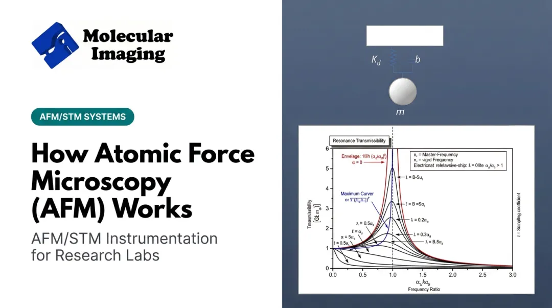
Measuring that tiny movement is the clever part. A laser reflects off the back of the cantilever onto a split photodiode detector; as the cantilever bends, the reflected spot moves, and the detector converts that shift into a precise deflection signal.
Tuning fork and interferometric detection methods exist in some specialized systems, but optical-lever detection remains the dominant approach across most commercial AFMs, including Molecular Imaging's platforms.
The probe then scans in a raster pattern, line by line across the x-y plane, building the image row by row. Scan speed and tip geometry directly affect resolution here: a dull tip blurs fine features regardless of how carefully everything else is tuned, and scanning too fast can outpace the feedback loop's ability to track the surface accurately.
Regulation and Control
This is where AFM earns its precision. An electronic feedback loop continuously adjusts the z-height of the tip (or sample) to hold a constant setpoint, whether that's deflection in contact mode, amplitude in tapping mode, or frequency in non-contact mode.
Why does this matter so much? Without it, the tip would either crash into the sample or drift too far away to sense anything useful. For soft biological samples, this feedback control is what keeps forces low enough to avoid crushing delicate structures, while still tracking surface detail down to the nanometer.
Older open-loop scanner designs suffered from piezoelectric hysteresis and thermal drift, which distorted images and made pixel positions unreliable over long scans. Modern closed-loop systems measure actual scanner position rather than just commanding it, correcting for this drift and delivering far more accurate, repeatable topography.
Output and Result
Every z-height adjustment the feedback loop makes, recorded at each x-y point, gets compiled into a topographic map, typically displayed as a pseudo-colored height image or a 3D surface render.
Topography is only part of the story. Depending on the probe and mode selected, AFM can simultaneously capture:
- Magnetic domain structure, using MFM-10 cantilevers
- Surface potential and electrical properties, using EFM-10 cantilevers for KPFM
- Mechanical stiffness and adhesion, through force-volume mapping
Resolution ultimately determines how useful that output is for downstream analysis. A 2025 cross-disciplinary review reports typical AFM lateral resolution of 1 to 10 nanometers, with vertical resolution below 1 nanometer under standard conditions, though this varies with tip shape, scanner noise, and sample properties.
Purpose-built biological platforms can push further. Molecular Imaging's 5500 ILM PicoPlus BioAFM, for instance, is specified at 0.2 nm vertical resolution—enough to resolve individual protein structures in liquid.

Where Is AFM Used?
AFM typically enters a research workflow at a few clear points:
- Characterizing a new surface
- Running quality control on thin films or coatings
- Mapping nanoscale mechanical, electrical, or magnetic properties before or after other techniques
Environment matters a lot here. AFM performs well in:
- Ambient air, for general materials characterization
- Liquid, for biological samples that need to stay hydrated and functional
- Vacuum, for atomic-resolution studies free of contamination
Temperature-controlled stages extend that range further, supporting reactive gas studies and battery research. Molecular Imaging's environmental control accessories, including stages rated from -30°C to 250°C, let researchers track phase transitions and thermal behavior without switching instruments.
Usage patterns shift by sector:
- Semiconductor and materials R&D labs lean on AFM for defect analysis and surface roughness measurement on wafers, thin films, and coatings
- Life-science labs use BioAFM systems such as the 5500 ILM PicoPlus BioAFM with liquid cells and MAC Mode cantilevers to image proteins, living cells, and membranes without fixing or coating
Traditional prep methods can distort or kill biological samples before you ever get an image. Liquid-cell AFM avoids that problem, imaging structures in near-native conditions.
Conclusion
AFM's strength comes from a mechanical probe, a sensitive detector, and a feedback loop working together. That combination traces surface features that light and electron beams cannot resolve at the same scale—and it is why AFM still opens new applications decades after its invention.
Understanding this working principle pays off practically. Knowing which mode fits your sample, and how feedback control affects image quality, helps you choose the right system or troubleshoot problems when images don't look right. Molecular Imaging's technical support team and ZoomAFM service can help with both—configuring a new modular system or keeping an existing AFM or STM running smoothly.
Frequently Asked Questions
How much does an atomic force microscope cost?
Pricing depends heavily on modularity, imaging modes, scan range, and accessories, so there's no fixed number. Contact Molecular Imaging for a configuration-based quote.
How long does atomic force microscopy take?
A single scan typically takes a few minutes to tens of minutes, depending on scan area, resolution, and mode. High-speed scanners can shrink this to under a minute for smaller images.
What is an atomic force microscope used for?
AFM is used for semiconductor surface and defect analysis, polymer mechanical characterization, operando battery research, and biological imaging of proteins, cells, and membranes.
What is the difference between AFM and STM?
STM measures tunneling current between a conductive tip and sample, so it only works on conductive materials. AFM measures mechanical force instead, allowing it to image virtually any surface, conductive or not.
Can AFM image samples in liquid or biological samples?
Yes. AFM in tapping or non-contact mode, especially with liquid cells and MAC Mode probes, images live cells, proteins, and membranes in liquid without special coatings or fixation.
What resolution can an atomic force microscope achieve?
Typical performance is 1 to 10 nm lateral resolution and below 1 nm vertically. Specialized systems and sample conditions can push vertical resolution finer still.