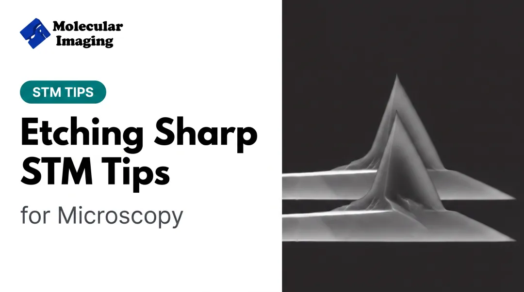
That's a mistake. A single-atom apex is what actually determines whether you get atomic resolution or a blurry mess of streaks and ghosts.
This guide covers what makes a good tip, how to choose the right material, how etching works, how to keep tips sharp longer, and how to troubleshoot the artifacts that show up when things go wrong. It's written for surface-science labs, electrochemistry groups, and molecular electronics researchers who depend on nanoscale precision every day.
Key Takeaways
- Tip condition — not scanner quality — is usually the biggest lever on STM resolution
- Tungsten suits vacuum work; Pt/Ir suits ambient and electrochemical environments
- Electrochemical etching remains the standard, low-cost path to atomically sharp tips
- Regular inspection and proper storage prevent streaking, doubling, and feedback instability
- Sourcing pre-tested tips and accessories (Molecular Imaging's web store, for example) cuts downtime
What Makes a Good STM Tip
Tunneling current depends exponentially on tip-sample distance. A 1 Å change in separation can shift measured current by an order of magnitude, according to a 2016 surface-science reference on STM physics. That sensitivity is what makes atomic resolution possible. It is also what makes a sloppy tip so punishing.
A good tip needs four things:
- Conductivity — clean electrical path for tunneling current
- Mechanical rigidity — resists vibration and drift during scanning
- Chemical stability — resists oxidation or contamination in the working environment
- Apex sharpness — ideally a single atom or small cluster carrying most of the current
Here's the part researchers often miss: "sharp" doesn't mean the macroscopic wire shape. It means the atom or cluster at the very end that actually carries the current. A wire etched to a beautiful cone can still image poorly if a second atomic cluster sits close enough to compete for tunneling current.
Common Consequences of a Bad Tip
- Streaking across scan lines
- Doubled or tripled features (ghost images)
- Unstable feedback loop, sudden current jumps
- Reduced lateral and depth resolution
For reference, commonly cited STM performance benchmarks sit around 0.1 nm lateral and 0.01 nm depth resolution, per a University of Padua STM resource. Treat these as achievable targets, not guaranteed specs. Tip quality is the variable that decides whether you get anywhere close.

Choosing the Right Tip Material
Material choice is a junction-design decision, not a hardness contest. It should match your environment: vacuum, ambient air, liquid, or low temperature.
| Material | Best for | Notes |
|---|---|---|
| Tungsten (W) | UHV, vacuum imaging | Easy to etch sharp; oxidizes readily |
| Pt/Ir | Ambient, electrochemical STM | Chemically inert; harder to fabricate |
| Gold (Au) | Molecular electronics, chemical-contrast work | Niche use; can be chemically modified |
| PtRh | Specialty applications | Limited published STM-specific data |
Tungsten tips dominate UHV work because they're straightforward to etch into extremely sharp cones. The catch: they form an oxide layer during etching that must be removed before use, often through UHV annealing or acid cleaning.
Pt/Ir tips are the standard choice for ambient and electrochemical STM. They resist the oxide problems that plague tungsten, which matters a lot when you're working in air or liquid electrolyte.
Molecular Imaging's web store carries both an etched Pt/Ir tip (PT-10), built for atomic-scale imaging and spectroscopy, and an insulated Pt/Ir tip rated below 70 pA for electrochemical measurements where controlling tunneling current matters.
Gold tips show up in molecular electronics and chemical-contrast experiments where the tip itself becomes part of the chemistry.
PtRh tips exist in some labs, but there isn't strong published STM-specific evidence backing general claims about them. Treat any PtRh recommendation as lab-specific until proven otherwise.
How STM Tips Are Made: Etching Techniques
The most common method is electrochemical (DC) etching: dip a wire into an etchant, apply voltage, and let the reaction dissolve the wire until it separates.
Two configurations dominate:
- AC droplet-etch method — commonly used for tungsten, relies on a meniscus at the air-electrolyte interface
- Lamella drop-off method — a double-lamella variant reported in a 2012 study produced larger cone angles and higher tip-quality yield than conventional single-lamella setups
Why Cutoff Timing Matters
The moment the wire separates, the circuit needs to shut off immediately. A 1990 tungsten-etching study in the Journal of Vacuum Science & Technology A found that cutoff times as fast as 500 nanoseconds produced tip radii from about 20 nm to over 300 nm, depending on circuit response. Miss that window and the freshly formed apex gets blunted by continued etching.
A typical tungsten protocol from Boston College uses 0.25 mm wire, a stainless-steel cathode, 2 M NaOH, and roughly 9-11 volts across a 15-20 minute cycle. These numbers work for that specific setup. They are not universal settings to copy blindly.
DIY etching setups have gained traction in some labs. A 2015 study using an Arduino Uno to control AC pulses reported atomic-resolution images from at least 70% of tungsten tips and 80% of Pt/Ir tips. That is a credible starting point, but reproducibility still depends on tight current monitoring and consistent etchant concentration—variables that are easy to get wrong without careful process control.

For that reason, many labs skip in-house fabrication entirely. Etching setups take time to dial in, and even well-documented protocols produce inconsistent yields without careful current control. Sourcing pre-etched, quality-tested tips saves that setup time and removes a variable from your imaging results.
Tips for Maintaining Sharpness and Extending Tip Life
A sharp tip won't stay sharp without basic care. Build these habits into routine tip handling:
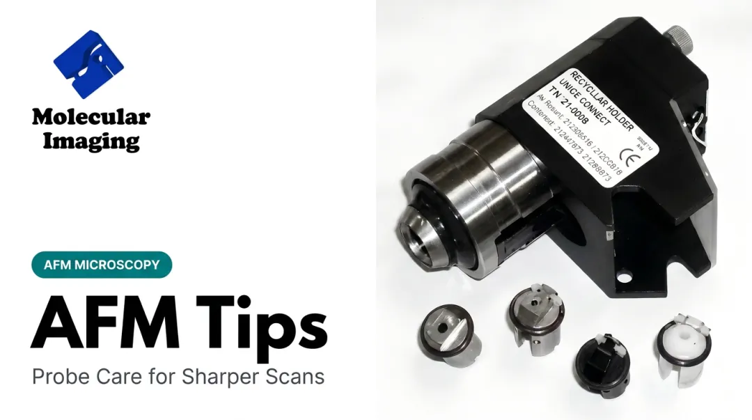
- Store tips clean and dry: keep them in a vibration-free, low-humidity environment to limit oxidation and dust
- Handle with proper tools: use tweezers and gloves, never bare fingers—skin oils contaminate the apex instantly
- Inspect periodically: check under optical or SEM magnification when unexplained artifacts appear in scans
- Keep a tip-change log: record age and handling history so problems map to a specific tip, not guesswork
In-Situ Conditioning
Voltage pulsing and controlled tip "crashes" can reshape a degraded apex without full replacement. High-field pulsing can move or eject surface atoms and reform the tip, but it is destructive by nature. Always run it away from your data region—ideally in a scan corner or a sacrificial clean area more than 100 nm off.
Controlled poking into a clean reference substrate works similarly: it strips contamination and sometimes re-coats the tip with fresh substrate atoms. Either way, condition only on a disposable area, then validate with a known reference image before trusting new data.

Troubleshooting Common Tip-Related Imaging Problems
Most STM artifacts trace back to one of two root causes: multiple apexes or contamination.
Multi-apex tips produce duplicated or "ghost" features: the same surface feature appears twice, offset by a fixed distance. Signs include:
- Repeated structures with consistent spacing
- More than one atomic cluster carrying current
Contaminated tips look different. Common symptoms:
- Unstable feedback or excess noise
- Sudden current jumps unrelated to the surface
Rule out scan speed, loop gain, and vibration isolation before blaming the sample.
The fastest fix in either case is usually a fresh or freshly conditioned tip. If conditioning does not resolve the issue, or you are burning through tips faster than expected, replace the tip rather than troubleshooting indefinitely.
Molecular Imaging's web store stocks etched and insulated Pt-Ir tips plus calibration samples such as gold-on-mica substrates, useful for validating a tip before you commit it to real data.
Frequently Asked Questions
What does STM stand for?
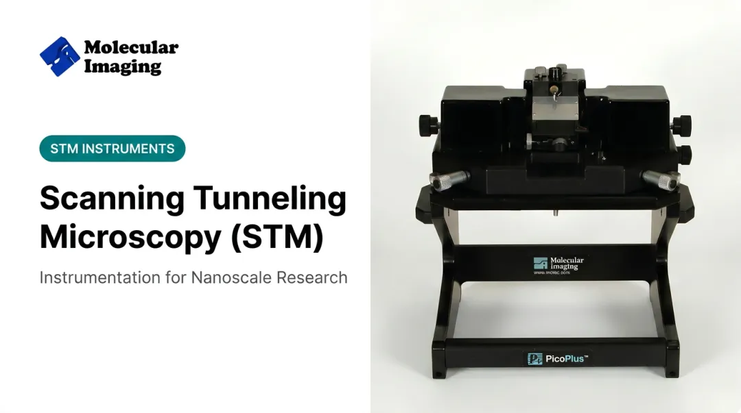
STM stands for Scanning Tunneling Microscope (or Microscopy): a technique that uses quantum tunneling current between a sharp conductive tip and a conductive sample to produce atomic-resolution images.
What is STM used for?
STM is used for surface defect analysis, semiconductor research, catalysis studies, and nanoscale lithography. It's also central to molecular electronics research involving charge transport at the nanoscale.
How does STM work?
A conductive tip is brought within a few angstroms of a conductive sample, and a bias voltage drives tunneling current across the gap. A feedback loop adjusts tip height via piezoelectric actuators to maintain constant current, and that height data builds the image.
What is the difference between STM and AFM?
STM requires a conductive sample and measures tunneling current across the tip-sample gap. AFM measures physical force between a cantilever and the sample, so it works on conductive and non-conductive surfaces alike.
How often should STM tips be replaced?
There's no fixed schedule. Replacement frequency depends on usage intensity, sample type, and how quickly image quality degrades. Watch for streaking, ghosting, or feedback instability as your signal to swap tips.
Can I make my own STM tips at home?
Yes, DIY electrochemical etching is well-documented and achievable with careful current control and consistent etchant concentration. Professionally sourced tips typically deliver more consistent research-grade imaging without the setup time.