Atomic force microscopy (AFM) has become the go-to tool for this kind of characterization, but there's a catch. A roughness value like Sa = 0.5 nm means nothing on its own. Without knowing the scan size, tip geometry, and processing steps behind that number, you can't trust it or compare it to anything else.
This guide walks through how AFM actually measures roughness, what factors distort your results, and how to choose an instrument and workflow that produces reproducible data.
Key Takeaways
- AFM maps height at nanometer to sub-nanometer resolution, far beyond optical or stylus profilers.
- Ra/Rq describe line profiles; Sa/Sq describe areal (3D) data — don't mix them when comparing results.
- Tip sharpness, scan size, and leveling can shift measured roughness by 10% or more.
- Use ISO 25178-2 when reporting areal (3D) surface texture parameters.
What Is Surface Roughness and Why Measure It With AFM
Surface roughness describes how far a surface deviates from its ideal flat form, once you've stripped away overall tilt and large-scale waviness. Those deviations drive real functional outcomes:
- Semiconductors: short-wavelength roughness on silicon wafers has been directly linked to electron-mobility degradation in MOSFETs.
- Coatings: roughness affects adhesion, wear resistance, and optical properties.
- Biomaterials: membrane and cell-surface texture can indicate cell health and influence fouling behavior.
AFM resolves features that optical and stylus profilers cannot reach. NIST describes AFM as capable of subnanometer imaging, which matters when you're characterizing post-anneal wafers with Sq values around 0.05 nm.
Roughness data from AFM feeds quality control decisions on production lines, supports R&D comparisons between material batches, and helps root-cause failure analysis when a device underperforms.
How AFM Measures Surface Roughness
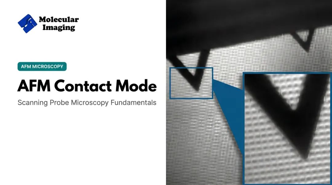
An AFM cantilever with a sharp tip scans across your sample. Tip-sample forces bend or vibrate the cantilever. A laser reflected off the cantilever’s back tracks that motion, and a feedback loop adjusts vertical position to hold a constant setpoint. The output is a three-dimensional height map of the surface.

Roughness Parameters: Ra, Rq, Sa, Sq
Once you have a height map, several standard parameters quantify texture:
| Parameter | Type | Definition |
|---|---|---|
| Ra | Profile | Mean absolute deviation from the mean line |
| Rq | Profile | Root-mean-square (RMS) deviation |
| Sa | Areal | 3D equivalent of Ra |
| Sq | Areal | 3D equivalent of Rq |
Rq weights larger height excursions more heavily than Ra, since it squares each deviation before averaging. Two surfaces with identical Ra can have very different Rq values if one has occasional tall spikes.
Two additional parameters add texture insight beyond basic roughness:
- Skewness (Ssk) distinguishes peak-dominated surfaces from pit-dominated ones
- Kurtosis (Sku) describes how sharp or heavy the peaks and valleys are
The Measurement Workflow
- Mount the sample flat, clean, and secured against drift
- Select a tip matched to feature size and required resolution
- Choose scan area and pixel density for the spatial wavelengths you need
- Acquire the image in tapping, contact, or non-contact mode
- Process the data with leveling, flattening, and parameter extraction

One caveat matters most after parameter extraction: roughness values are scale-dependent. A 1×1 µm scan and a 10×10 µm scan of the same surface will report different Sq values because they sample different spatial wavelengths. Always document scan size and pixel matrix with every reported number.
Factors That Affect Measurement Accuracy
Even a well-calibrated AFM can produce misleading roughness numbers if you overlook a few key variables.
Tip Sharpness and Convolution
The tip has a finite apex radius, so what you're really recording is a geometric convolution of tip and sample shape. A sharper probe, such as Molecular Imaging's SSS-NCHR super-sharp cantilever, resolves finer features and typically yields higher apparent roughness than a standard tip on the same surface. Narrow features can appear widened or merged with a blunter tip, distorting your lateral measurements.
Leveling and Line Correction
Plane leveling, polynomial bow removal, and line-by-line correction are necessary to strip out scanner artifacts. But research shows these same steps can underestimate roughness by 5-30% depending on the method used, particularly when scan size is small relative to the surface's correlation length (Nečas et al., 2020).
Practical fix: keep raw, leveled, and corrected versions of every image. Compare roughness values at each stage. If leveling swings your Sq by 20%, flag that in your report rather than hiding it.
Watch for These Artifacts
- Tip convolution: distorts lateral feature size and apparent roughness
- Feedback oscillation: introduces false height variations
- Scan drift: thermal or mechanical shifts during acquisition, sometimes ~20 nm on the slow-scan axis
- Trace/retrace mismatch: large disagreement between forward and backward scans signals a setup problem
Never compare roughness between samples unless scan sizes, regions, and preprocessing steps match. An Sa value from a 2×2 µm scan is not comparable to one from a 20×20 µm scan.
AFM vs. Other Surface Roughness Measurement Techniques
AFM isn't always the right tool. Here's how it stacks up against the alternatives:
| Factor | AFM | Optical/Stylus Profilometry |
|---|---|---|
| Resolution | Sub-nanometer, small field of view | Larger area, lower resolution ceiling |
| Data type | Full areal (3D) topography | Often line-profile or lower-density 3D |
| Speed | Slower: one comparison found roughly 250 seconds per image | Much faster: around 12 seconds per image in the same study |
| Sample contact | Gentle; tapping mode reduces shear force | Stylus is direct contact and can damage soft surfaces |
| Environment | Works in air or liquid | Typically limited to air-dried samples |

A 2023 comparison study found that while both methods produce usable 2D and 3D topography, AFM delivered noticeably higher resolution and precision at the nanoscale, at the cost of throughput.
When to choose which: if you're characterizing ultra-smooth or nanoscale surfaces where sub-nanometer detail matters, AFM wins. If you need to screen large areas quickly and nanometer precision isn't critical, optical or stylus methods make more sense.
Applications Across Research and Industry
AFM roughness measurement shows up across a wide range of research and industry settings:
- Semiconductor wafer and thin-film QC: 1×1 µm² AFM scans have tied short-wavelength roughness (Sq near 0.05 nm post-anneal) directly to device-level electron mobility, supporting process diagnosis at a scale no other technique reaches.
- Coatings and thin films: Studies on Si/Cr, Si/Ni, Si/Ti, and Si/Pt films report RMS roughness from roughly 0.3 nm to 2.7 nm depending on deposition method.
- Batteries: Electrode roughness affects zinc stripping/plating stability during cycling; a mid-roughness surface supported over 1,000 hours of cycling in one study. Electrochemical AFM (EC-AFM) watches these interfaces evolve in real time.
- Life sciences: Liquid-cell AFM images cell membranes, DNA, and proteins in their native hydrated state. One study found RMS values around 1.07 nm for DNA microarray probe regions versus 0.429 nm for silanized glass, enough to separate functional biomolecular surfaces from bare substrate.
Choosing the Right AFM System and Support for Roughness Studies
Roughness studies rarely happen in isolation. A lab characterizing thin films this week might need particle analysis or mechanical property mapping next month. Reconfiguring an entire instrument for every project wastes time and money.
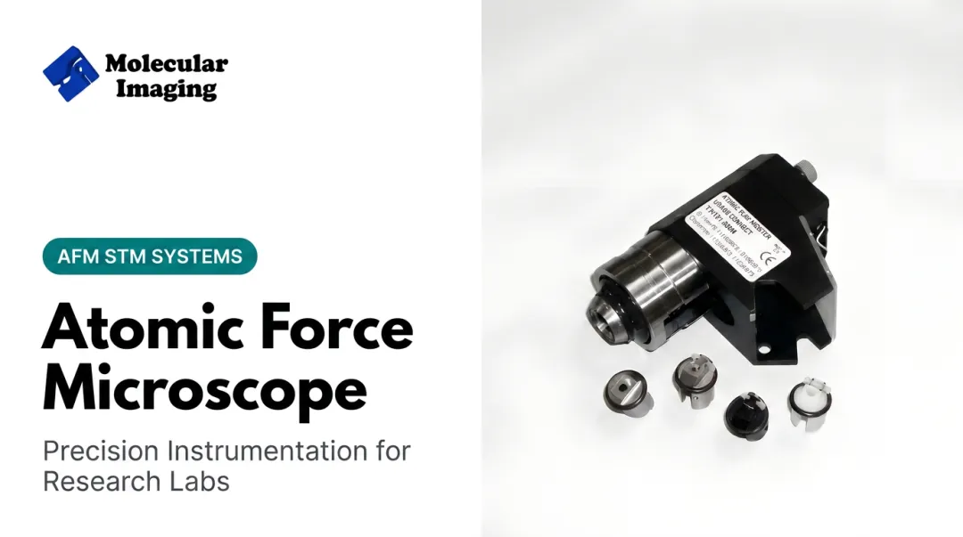
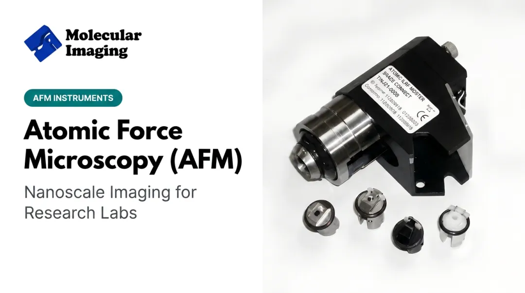
Modular architecture addresses that constraint directly. Molecular Imaging's PicoPlus platforms use a pendulum-style multipurpose scanner with interchangeable nose cones. Researchers can switch between AFM imaging, STM, and force-measurement configurations without replacing the whole microscope. Scan ranges span from 9×9 µm for atomic-resolution work up to 90×90 µm for broader surface or particle imaging, covering both fine roughness detail and larger-area statistical sampling in one system.

For roughness work specifically, a few features matter most:
- Closed-loop scanning to reduce positioning distortion during piezoelectric movement
- Low-noise electronics and rigid mechanical design to minimize drift-related artifacts
- Environmental isolation and temperature-controlled stages (Molecular Imaging's range from -30°C to 250°C) to keep thermal drift from corrupting height data
- Liquid-cell compatibility for membrane, protein, and electrochemical roughness studies
Labs running older or malfunctioning AFM/STM systems don't need to replace the whole instrument to get reliable data back. Molecular Imaging's ZoomAFM service handles diagnosis, scanner calibration, and controller-electronics repair using platform-matched parts, which helps restore the measurement stability that accurate roughness reporting depends on.
Beyond the instrument itself, a dependable roughness workflow needs supporting infrastructure:
- Calibration samples: 500 nm grating standards and gold-on-mica substrates to verify performance before you trust the numbers
- Probe selection guidance: match cantilever sharpness (such as the SSS-NCHR super-sharp probe) to your feature scale
- Installation and calibration docs: scanner procedures, alignment guides, and controller setup videos that keep results reproducible across users
Careful technique still matters. Pair it with modular hardware, verified calibration references, and responsive repair support, and the roughness values you publish become much easier to defend.
Frequently Asked Questions
What can an AFM measure?
AFM measures surface topography and roughness, along with mechanical properties like stiffness and adhesion. Depending on the mode used, it can also capture electrical and magnetic surface properties.
What is the standard for surface roughness?
ISO 25178-2 is the recognized international standard for areal surface texture parameters, including Sa, Sq, Ssk, and Sku. It defines terminology and parameter calculations for 3D surface data.
What is the difference between Ra and Rq in AFM roughness measurement?
Ra is the mean absolute deviation of surface height from the mean line. Rq is the root-mean-square deviation, which weights larger height excursions more heavily than Ra does.
Why does AFM roughness change with scan size?
Different scan sizes sample different spatial wavelengths on the surface. A small scan may miss long-wavelength features, while a large scan averages out fine detail, making roughness inherently scale-dependent.
Does the AFM tip affect roughness results?
Yes. Sharper tips resolve finer surface features and typically produce higher measured roughness than standard tips scanning the same surface, since blunter tips smooth over small peaks and valleys.
How do I choose between AFM and optical profilometry for roughness measurement?
Choose AFM for nanoscale or ultra-smooth surfaces where sub-nanometer detail matters. Choose optical profilometry when you need faster measurements over larger areas and nanometer precision isn't essential.