Introduction
In 1981, two IBM physicists in Zurich built an instrument that could see individual atoms without a single photon or electron beam. Scanning tunneling microscopy (STM) relies on a quantum phenomenon: electrons tunneling across a gap they classically shouldn't cross.
That discovery earned Gerd Binnig and Heinrich Rohrer the 1986 Nobel Prize in Physics and opened the door to modern nanotechnology.
Researchers new to nanoscale characterization often lump STM together with scanning electron microscopy (SEM) or atomic force microscopy (AFM). The three techniques solve different problems, and picking the wrong one wastes time and sample prep.
This guide breaks down how STM works, the hardware behind it, and where it fits against SEM and AFM. It also covers research applications—from semiconductor defect mapping to molecular electronics—where tunneling-based imaging is the right tool for the job.
Key Takeaways
- Quantum tunneling between a sharp tip and sample delivers atomic and sub-angstrom resolution
- Conductive or semiconducting samples only; AFM covers nearly any material instead
- Constant-current mode dominates labs; constant-height mode trades tip safety for speed
- Core uses span semiconductors, electrochemistry, molecular electronics, and monolayers
- Scanning tunneling spectroscopy (STS) maps electronic states, not surface topography
What is Scanning Tunneling Microscopy?
Scanning tunneling microscopy was the first scanning probe microscopy technique ever built. Physicists Gerd Binnig and Heinrich Rohrer invented it in 1981 at the IBM Research Laboratory in Zurich, Switzerland. Five years later, the Nobel committee awarded them half of the 1986 Nobel Prize in Physics "for their design of the scanning tunnelling microscope."
Before STM, nobody had directly visualized individual atoms on a surface. Electron microscopes came close, but their beams could damage delicate samples and still couldn't pin down atomic positions with certainty. STM changed that by measuring a tunneling current instead of bouncing light or electrons off a sample. Interatomic spacing on conductive surfaces suddenly became visible, then controllable.
That control turned STM into more than an imaging tool. IBM researchers famously used a low-temperature STM to drag individual xenon atoms across a nickel surface, spelling out "IBM" one atom at a time. A separate IBM team later arranged 48 iron atoms into a circular "quantum corral," trapping electron waves inside it like ripples in a pond. That experiment proved STM could probe and shape matter at the atomic scale at the same time.
This dual capability is why STM is often credited as the technique that launched modern nanotechnology:
- Direct visualization of atomic-scale surface topography on conductive materials
- Deliberate repositioning of individual atoms
- Foundation for scanning probe microscopy, including later AFM development
How Does Scanning Tunneling Microscopy Work?
STM combines three things working together in real time: a quantum mechanical effect, a piezoelectric positioning system precise to fractions of an angstrom, and a feedback loop fast enough to react to atomic-scale surface bumps before the tip crashes. Here's how the physics, imaging modes, hardware, and operating environments fit together.
Quantum Tunneling: The Physics Behind STM
Electrons don't behave like tiny billiard balls. They behave like waves, which lets them pass through barriers that classical physics says should stop them cold. That's quantum tunneling, and it's the entire physical basis for STM.
When a sharp conductive tip approaches a conductive sample, typically within less than a nanometer, and a small bias voltage is applied between the two, electrons tunnel across the gap even without physical contact. That flow of electrons is the tunneling current STM actually measures.
This current is extraordinarily sensitive to distance. It decays exponentially as the gap widens: a study in the Journal of Physical Chemistry C measured roughly a 10-fold increase in tunneling current for every 1 angstrom decrease in tip-sample separation. That relationship is why STM can resolve height changes as small as picometers, far below what any optical or electron-based method can detect.
Two Imaging Modes: Constant Height vs. Constant Current
STM images come from one of two operating modes, and the right choice depends on how flat the sample is and how fast you need to scan.
Constant current mode is the default for most labs. A feedback loop continuously adjusts tip height to keep tunneling current fixed at a set value.
The system records that height at every point, building a 3D map that blends surface topography with local electronic density of states. Because the tip physically retreats over bumps, this mode tolerates rougher surfaces without crashing.
Constant height mode skips the feedback loop entirely. The tip stays at a fixed vertical position while current fluctuations are recorded directly. It's considerably faster, sometimes running at frequencies up to 10 kHz, but it only works safely on atomically flat samples.
| Mode | Speed | Best for | Main risk |
|---|---|---|---|
| Constant current | Standard | Rough or unknown surfaces | Minimal |
| Constant height | Fast | Atomically flat samples | Tip crash |
Most researchers default to constant current simply because it's more forgiving. Surface features large enough to exceed a preset gap can destroy a tip in constant-height operation.
Core Components of an STM System
Every STM, regardless of manufacturer, relies on the same core hardware stack:
- A sharp conductive tip, usually tungsten or platinum-iridium (Pt-Ir), often electrochemically etched to a fine apex
- Piezoelectric scanners for x, y, and z positioning, accurate to fractions of an angstrom
- Feedback electronics that monitor tunneling current in real time and adjust tip height accordingly
- Vibration and acoustic isolation, since the current being measured is often just picoamps

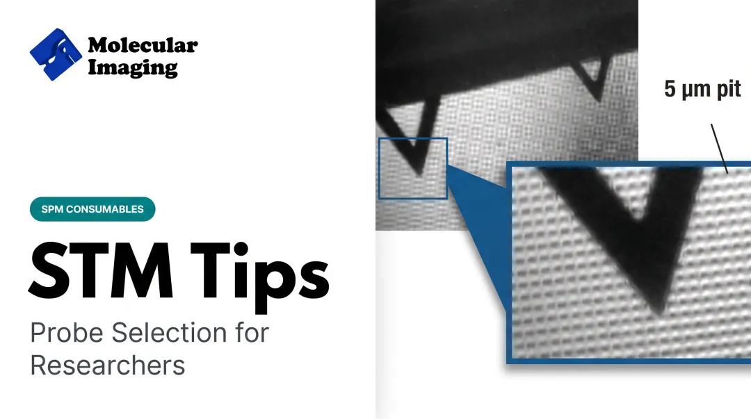
Tip choice matters more than most newcomers expect. Molecular Imaging sells both etched and insulated Pt-Ir tips for this reason: etched tips maximize resolution for standard surface imaging, while insulated variants confine the tunneling current to the very apex.
That confinement matters in electrochemical STM, where stray Faradaic current would otherwise swamp the signal. Insulated tips with a defined current threshold under 70 pA run around $10 each, cheap insurance against a ruined dataset.
Modular instrumentation changes how labs use this hardware day to day. Platforms like Molecular Imaging's 5500 PicoPlus AFM+STM and 5420 PicoAFM use interchangeable nose cones, so a researcher can switch between STM, contact AFM, tapping mode, and other techniques on the same scanner.
The dedicated 4500 PicoSTM serves labs that only need tunneling-based imaging without the added AFM hardware.
Operating Environments: Ambient vs. Ultra-High Vacuum (UHV) STM
STM systems generally fall into two environmental categories, and the choice affects both what you can study and what the setup costs.
Ambient STM runs in air, controlled gas, or liquid, usually near room temperature. It's the practical choice for electrochemical STM, in-situ reaction monitoring, and any experiment where pumping down to vacuum isn't feasible.
Molecular Imaging builds ambient STM into its modular 5500 PicoPlus and PicoAFM platforms. Those systems pair with environmental isolation chambers for humidity, gas, and low-oxygen control, plus temperature-controlled stages spanning -30°C to 250°C for phase-transition and thermal studies.
Ultra-high vacuum (UHV) STM sits at the other extreme. Some UHV instruments operate below 1 K for spectroscopy on superconductors, while specially designed environmental STMs can push toward 1,300 K on the high end, though no single system spans that entire range. UHV removes surface contamination that would otherwise obscure atomic-scale features, making it standard for fundamental surface-science work.
Neither environment is universally better. Ambient and liquid-cell STM suit electrochemistry, battery research, and molecular electronics work where reactions need to happen under real conditions. UHV suits ultra-clean semiconductor and superconductor studies where a single stray molecule can throw off a measurement.
Scanning Tunneling Microscopy vs. SEM and AFM: Key Differences
Researchers new to nanoscale imaging often default to whichever microscope their lab already owns. That choice fails when the sample or research question doesn't match the technique.
STM vs. SEM
Scanning electron microscopy (SEM) scans a focused electron beam across a sample and measures the electrons that bounce back or are emitted. It requires vacuum and can image both conductive and non-conductive samples, though non-conductors often need a conductive coating first. Typical resolution reaches a few nanometers.
STM works differently. It measures tunneling current rather than reflected electrons, requires a conductive or semiconducting sample with no coating, and achieves atomic resolution: roughly 2 angstroms laterally and 0.1 angstrom vertically, per the Nobel record cited above. SEM shows shape and morphology at the nanoscale; STM shows individual atoms.
STM vs. AFM
Atomic force microscopy (AFM) measures physical force between a cantilever tip and the sample rather than electrical current. That's the key difference: AFM works on virtually any material, conductive or not, biological or inorganic, in air or liquid. STM only works on samples that conduct electricity well enough to sustain a tunneling current.
In exchange for that limitation, STM offers something AFM can't: direct access to electronic structure. Because tunneling current depends on local density of electronic states, not just physical height, STM (and especially STS) reveals molecular orbitals, band gaps, and quasiparticle behavior that force-based measurement doesn't capture.

Quick decision guide:
- Sample doesn't conduct electricity: choose AFM
- Need topography plus electronic structure on a conductive sample: choose STM
- Need atomic resolution on almost any material: AFM in suitable modes, tip-dependent
- Working in vacuum across mixed conductive and non-conductive regions: SEM for overview, STM for atomic detail on conductive areas
Many labs want both capabilities without buying two separate instruments. That demand is why combined AFM/STM platforms are common in shared research facilities.
Applications of STM in Research
STM's impact spans across nanoscale research, from basic surface science to commercial semiconductor fabrication.
Surface structure and defects. The technique's first major scientific result came in 1983, when Binnig and Rohrer's team resolved the Si(111)-7×7 surface reconstruction in real space, confirming a 12-adatom-per-unit-cell model that had been debated for years. STM remains a standard tool for mapping atomic-scale defects and reconstructions on metals and semiconductors used in electronic component fabrication.
Nanofabrication. Beyond imaging, STM can physically manipulate atoms and molecules. The quantum corral experiment, where researchers arranged 48 iron atoms on copper and captured the resulting electron-wave interference, remains a landmark demonstration of atom-by-atom construction. Related techniques have since enabled:
- Prototype molecular switches
- Patterned metal contacts on nanodevices
- Controlled placement of single atoms and molecules
Self-assembled monolayers and single-molecule imaging. STM resolves sub-molecular detail in organic films on graphite (HOPG), revealing how individual molecules pack and orient within a monolayer. Molecular Imaging's examples include C60 molecular structures on HOPG and atomic-lattice resolution on bare HOPG with the 5500 PicoPlus AFM+STM. Datasets like these need a stable tip and a well-characterized substrate.
Electrochemistry and molecular electronics. In-situ electrochemical STM (EC-STM) lets researchers watch surface reactions happen in real time, tracking copper deposition or crystal growth at an electrode interface instead of reconstructing it later. Molecular electronics researchers use similar setups to study charge transport through molecular junctions, work that depends on insulated STM tips to keep stray current from contaminating the measurement.
For labs running these experiments daily, uptime matters as much as resolution. Molecular Imaging's ZoomAFM service covers diagnostics, calibration, and hardware repair for aging AFM/STM systems, with remote troubleshooting and on-site visits when video support isn't enough. Replacing a legacy STM is expensive; servicing one that already produces good data is often the smarter path.

Scanning Tunneling Spectroscopy (STS): Beyond Topography
Standard STM tells you where atoms sit. Scanning tunneling spectroscopy (STS) tells you what those atoms are doing electronically, using the exact same hardware.
How STS Differs from STM Imaging
Instead of scanning across a surface, STS holds the tip fixed above one point, disables the height feedback loop, and sweeps the bias voltage while recording current. The resulting differential conductance curve maps the local density of electronic states at that atomic location.
That spectrum reveals molecular orbitals, band gaps, and electron behavior topographic imaging alone can't provide. Repeating the measurement across a grid builds a full electronic map of a region, not just a single-point spectrum.
Where STS Gets Used
- Superconductor research — maps how zinc impurity atoms locally disrupt superconductivity and create quasiparticle-scattering signatures at each defect
- Semiconductor band structure — characterizes surface band gaps, though quantum confinement can shift apparent edges from true intrinsic values
- Quasiparticle interference — uses energy-dependent conductance modulations to probe electronic structure in high-Tc superconductors atom by atom
For molecular electronics and materials science, STS adds something AFM can't replicate: point-specific electronic fingerprinting on the same sample just imaged for topography. One instrument producing two complementary data types is why AFM/STM platforms with STS remain staples in labs studying charge transport and electronic materials.
Frequently Asked Questions
What is the difference between scanning tunneling microscopy (STM) and scanning electron microscopy (SEM)?
STM uses tunneling current between a conductive tip and sample for atomic-resolution imaging of conductive surfaces. SEM scans a focused electron beam and can image conductive or non-conductive samples, but without true atomic resolution.
How does scanning tunneling spectroscopy work?
STS holds the tip stationary above a chosen point, sweeps the bias voltage, and measures how current changes. That data maps the local density of electronic states at that specific atomic site.
Can STM be used to image non-conductive materials?
No. STM depends on tunneling current, which requires a conductive or semiconducting sample. Non-conductive materials are better suited to AFM, which measures force rather than current.
What is the difference between STM and AFM?
STM measures tunneling current between tip and sample and is limited to conductive or semiconducting surfaces. AFM measures tip-sample force or cantilever deflection, so it works on nearly any material—including insulators, polymers, and biological samples.
What resolution can scanning tunneling microscopy achieve?
STM routinely resolves features below 0.1 nm laterally and around 0.01 nm (10 pm) vertically, precise enough to image and manipulate individual atoms.
Does STM require ultra-high vacuum to operate?
Not always. Many STMs run in UHV for maximum stability and temperature range, but ambient STMs also operate reliably in air, gas, or liquid near room temperature.