Introduction
A battery cell fails or thrives at a boundary you can't see: the electrode-electrolyte interface. A catalyst's efficiency lives in a layer of atoms just a few nanometers thick. Corrosion, protein folding, semiconductor performance — all of it happens at surfaces and interfaces.
Researchers know this. The problem is choosing the right tool. Surface science spans dozens of specialized instruments, from ultra-high vacuum spectroscopy chambers to scanning probes that work in a beaker of electrolyte. Picking the wrong instrument wastes months of grant money and lab time.
This guide breaks down what surface science instruments actually do, the major categories available, where each shines, and how to match an instrument to your research question.
Key Takeaways
- Surface science instruments resolve physical and chemical interface behavior that conventional microscopy misses
- Two main families: vacuum spectroscopies (XPS, AES, LEED) and ambient scanning probes (AFM, STM)
- AFM and STM enable nanoscale imaging, electrochemistry, and bioimaging without ultra-high vacuum
- Match the instrument to your sample type, resolution needs, and working environment
What Is Surface Science?
Surface science studies the physicochemical phenomena occurring at interfaces: solid-liquid, solid-gas, liquid-gas, and solid-vacuum boundaries. It sits at the intersection of physics and chemistry, and that split shows up in how researchers describe their work.
Surface chemistry covers catalysis, electrochemistry, and geochemistry (reactions on a surface). Surface physics covers phonons, plasmons, diffusion, and nanostructure formation (the physical behavior of that boundary layer).
From Vacuum Chambers to Living Cells
The field emerged as its own discipline between 1964 and 1973. Reliable ultra-high-vacuum (UHV) systems, operating at pressures below 10⁻⁷ Pa, combined with electron spectroscopy to make stable, reproducible surface measurements possible for the first time. A 2007 PNAS historical review traces this origin point directly to UHV technology paired with single-crystal samples.
That review also documents the field's second wave: extending analysis beyond vacuum into solid-liquid interfaces and fragile biological samples. Scanning probe microscopy (AFM and STM specifically) made this possible, generating atomic-scale images in vacuum, in liquid, and on biological specimens alike.
Surface analysis no longer requires a vacuum chamber. It now spans everything from single-crystal platinum in UHV to a living cell sitting in buffer solution.
Categories of Surface Science Instruments
Vacuum-Based Spectroscopy and Diffraction
These techniques require ultra-high vacuum and probe extremely shallow depths:
| Technique | What it measures | Typical depth |
|---|---|---|
| XPS | Photoelectron kinetic energy | ~1-10 nm |
| AES | Auger electron energy after electron excitation | 3-10 nm |
| LEED | Diffraction pattern from a focused electron beam (30-500 eV) | Surface order/symmetry |
| ISS/LEIS | Ion scattering | Outermost atomic layer |
| SIMS/ToF-SIMS | Mass-to-charge of sputtered secondary ions | 1-2 nm |
Vacuum techniques deliver high chemical specificity, but samples must survive vacuum for hours.
Optical and X-Ray Techniques
Surface-enhanced Raman, surface plasmon resonance (SPR), GISAXS, and GIXD probe interfaces under ambient or liquid conditions. SPR, for instance, tracks molecular binding in real time at a sensor surface — no vacuum needed, according to Harvard Medical School's Center for Macromolecular Interactions.
Scanning Probe Microscopy (SPM)
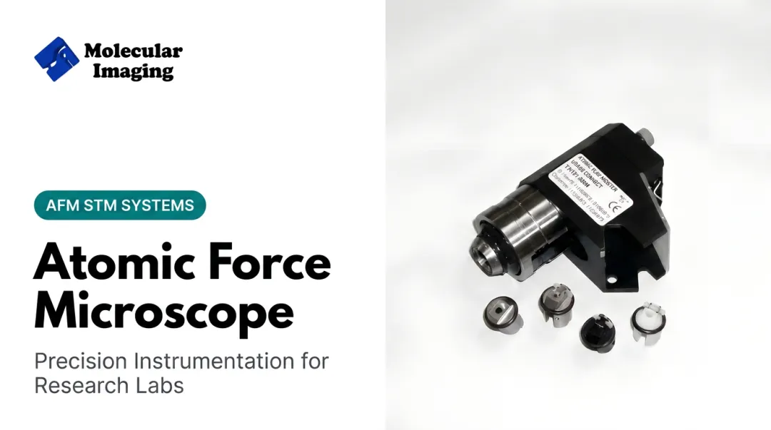
AFM and STM generate atomic-resolution images through direct physical interaction with a surface, not electron or photon scattering. Both can operate in air, vacuum, or liquid, which opens biological and electrochemical work that vacuum methods cannot support.
Why this matters for lab flexibility: modular AFM/STM systems let one platform serve multiple research programs. Molecular Imaging examples include:
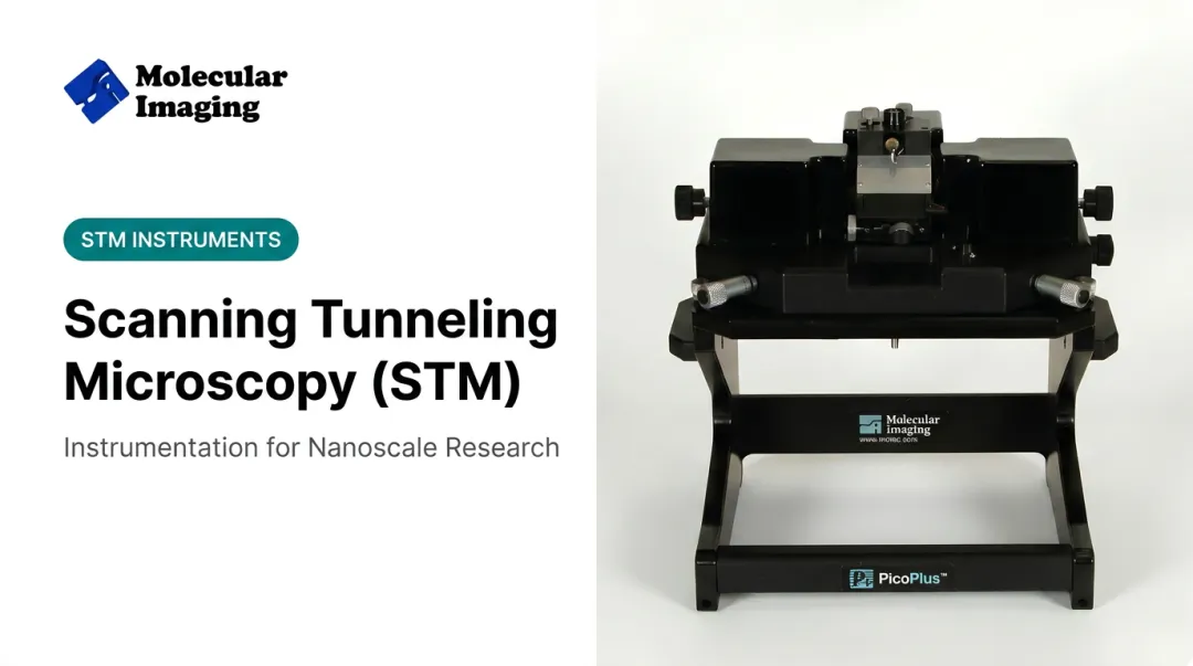
- 5500 PicoPlus AFM+STM: swappable nose cones for AFM, STM, conductive AFM, tapping mode, KPFM, EFM, and MFM, covering topography, electronics, and magnetic properties on one chassis
- 5420 PicoAFM: nose-cone swaps between AFM, STM, and force-measurement configurations, with scan ranges from 9 µm to 90 µm
That modularity means a materials lab studying thin films today can reconfigure the same instrument for electrochemistry or bio-imaging tomorrow, without buying a second system.

AFM vs STM: Key Differences
The two core scanning probe techniques rely on different physical principles.
STM measures the tunneling current flowing between a sharp conductive tip and the sample surface. That current only flows through conductive or semiconductive materials, which limits STM's sample scope but yields atomic-resolution images of metals, graphite, and semiconductors.
AFM measures cantilever deflection as a tip physically responds to surface forces. Because it doesn't rely on electrical current, AFM works on:
- Insulating materials
- Polymers
- Biological samples in liquid
- Virtually any surface, conductive or not
Combined AFM+STM platforms let researchers correlate physical topography (AFM) with electronic structure (STM tunneling current) on the same conductive sample. A system like the 5500 PicoPlus AFM+STM delivers both modes in one instrument, something neither technique provides alone.

Applications of Surface Science Instrumentation
Catalysis Research
Model catalyst surfaces, often single-crystal platinum, reveal how adsorption behavior drives real-world performance. A 2010 Lawrence Berkeley National Laboratory study used high-pressure STM to watch platinum terraces fracture into nanometer-sized clusters as CO coverage approached saturation. Those nanoclusters potentially outperformed the flat single crystal under catalytic conditions.
Electrochemistry
In-situ AFM and STM let researchers image electrode-electrolyte interfaces while a potential is actively applied. This isn't possible with vacuum techniques, since the electrolyte itself would destroy the vacuum.
Molecular Imaging's 5500 Series and 5420 PicoAFM support this work through liquid cells compatible with:
- Aqueous electrolytes
- Acidic and basic solutions
- Organic solvents
One documented example: imaging copper deposition on Au(111) in a sulfuric acid/copper sulfate solution, tracking distinct electrochemical features at specific applied voltages.
Materials Science
Thin-film and battery-electrode characterization benefit from AFM's mechanical and electrical sensitivity. A 2017 study in Scientific Reports used AM-FM AFM and Kelvin probe force microscopy to track LiCoO2 cathode grain growth over battery cycling. Grain size grew from roughly 96 nm to over 115 nm after 100 cycles, with roughness nearly doubling.
For this kind of work, cantilever choice matters:
- Contact-mode silicon cantilevers for grain-boundary topography
- Conductive contact cantilevers for simultaneous electrical mapping
- Liquid-tapping cantilevers for battery interfaces studied directly in electrolyte
Life Sciences (BioAFM)
AFM's biggest advantage in biology: no fixation, no staining, no vacuum. Researchers image samples in their native liquid environment.
Systems like the 5500 ILM PicoPlus BioAFM use MAC Mode, a magnetic AC tapping technique, to keep probe-sample forces gentle enough for live cells, proteins, and DNA. Documented case studies include living-cell imaging, chromatin structure, and sperm morphology, all captured in liquid at sub-angstrom lateral resolution.

Choosing the Right Surface Science Instrument for Your Lab
Before buying, work through these questions in order.
1. What environment does your sample need?
- Ambient air: AFM and many other SPM techniques
- Liquid: AFM/STM only (with liquid cells)
- Ultra-high vacuum: XPS, AES, LEED, ISS
2. What are you actually measuring?
- Topography → AFM
- Electronic structure → STM or XPS
- Chemical composition → XPS, AES, SIMS
- Ordering/crystallography → LEED, GIXD
3. Does your research need modularity? Labs juggling multiple projects (thin films one month, electrochemistry the next) benefit from swappable-configuration systems rather than single-purpose instruments. Temperature-controlled stages extending from -30°C to 250°C add another layer of flexibility for thermal or phase-transition studies.
4. What's your long-term support plan? Instruments age. Labs running legacy Agilent-era 5500 or 4500 systems should factor in service availability before it becomes an emergency. Molecular Imaging's ZoomAFM program provides diagnostics, calibration, and repair specifically for these legacy platforms, with both remote and on-site support options.
Frequently Asked Questions
What is surface science?
Surface science is the study of physicochemical properties at the boundary between two phases, such as solid-liquid or solid-gas interfaces. It bridges chemistry (reactions at surfaces) and physics (structural and electronic behavior).
What is the difference between AFM and STM?
STM measures tunneling current and works only on conductive or semiconductive samples. AFM measures cantilever deflection, so it can image insulators, soft matter, and biological samples in liquid.
What industries use surface science instruments?
Nanotechnology, materials science, life sciences, electrochemistry, and semiconductor research all rely on surface science tools. Applications range from battery R&D to catalyst design to protein imaging.
Do surface science instruments require a vacuum?
Some do. XPS and AES need ultra-high vacuum for stable measurements. AFM and STM do not; they run in air, vacuum, or liquid depending on the sample.
How do researchers maintain aging AFM/STM systems?
Legacy Agilent and Molecular Imaging systems often need specialized calibration and repair once the original manufacturer's service ended. ZoomAFM provides diagnostics, parts replacement, and remote or on-site repair for these platforms.