SCM combines AFM's mechanical positioning with a sensitive capacitance sensor, turning a metal-coated tip into one plate of a nanoscale capacitor. As the tip scans, it measures capacitance changes that reveal dopant concentration and carrier behavior invisible to topography alone.
That matters because semiconductor researchers need sub-10nm spatial resolution to keep pace with shrinking device features. NIST has flagged sub-10nm dopant metrology as a real requirement for modern device scaling, not a nice-to-have. This article breaks down what SCM is, how it works, where it's used, and what to look for in an AFM system built to run it.
Key Takeaways
- SCM maps dopant concentration, carrier type, and dielectric properties by measuring tip-sample capacitance at the nanoscale
- Best fit is semiconductor and MOS device characterization; resolution depends on tip geometry and local dopant concentration
- Setup requires a metal-coated probe, a dedicated capacitance sensor module, and a modular AFM that hosts the sensor
What Is Scanning Capacitance Microscopy (SCM)?
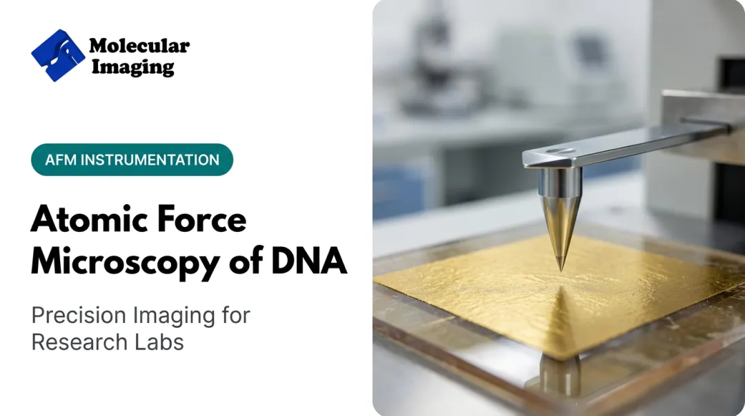
SCM is an AFM-based electrical mode, not a separate microscope. It layers a high-frequency capacitance measurement circuit onto standard AFM positioning, producing two data channels from a single scan: topography and capacitance. The key hardware difference is the probe. Standard AFM cantilevers won't work here: SCM requires a metal-coated tip, typically Pt/Ir or Co/Cr coated silicon, so it can act as one electrode in a tip-sample capacitor.
Why MOS Structures Are Central to SCM
SCM has a strong, specific association with metal-oxide-semiconductor (MOS) structures. The oxide layer isn't incidental; it's part of the measurement itself, forming one half of a series-capacitor model with the underlying semiconductor's depletion layer.
The Resolution Claim, Properly Sourced
You'll often see SCM described as capable of sub-10nm resolution. That figure traces back to a 2004 study in Review of Scientific Instruments reporting sub-10nm lateral resolution under specific probe conditions (tip size roughly matched to the target feature). The 2013 ITRS metrology roadmap lists SCM among dopant-profiling methods and notes that resolution depends heavily on dopant concentration, not a fixed instrument spec. Treat sub-10nm as a documented benchmark under stated conditions, not a guarantee across every sample and setup.
How Does Scanning Capacitance Microscopy Work?
At its simplest, SCM treats the tip and sample as two capacitor plates separated by a thin oxide dielectric.
The Dual-Electrode Model
An AC or DC voltage is applied through the conductive tip while the sample sits at (or near) ground. A high-frequency resonant circuit paired with a lock-in amplifier detects tiny capacitance changes as the tip scans. That output is the dC/dV signal, which varies across regions with different dopant concentrations.
Two Capacitors in Series
The measured capacitance isn't one value. It's a series combination:
- Oxide capacitance — fixed by oxide thickness and dielectric constant
- Depletion capacitance — variable, changes as the AC signal modulates the depletion width near the oxide-silicon interface
This series relationship (1/C_total = 1/C_oxide + 1/C_depletion) is why oxide thickness directly affects what you read as "carrier contrast."

What Happens Without an Oxide Layer
Oxide-free samples form a Schottky contact instead of a true MOS capacitor. Current can flow across this junction. Electron accumulation or depletion near the surface then changes the capacitance signal in ways that are harder to model cleanly than the insulated MOS case.
That distinction matters when you interpret results on bare semiconductor surfaces versus oxide-covered ones.
Where the AFM Part Comes In
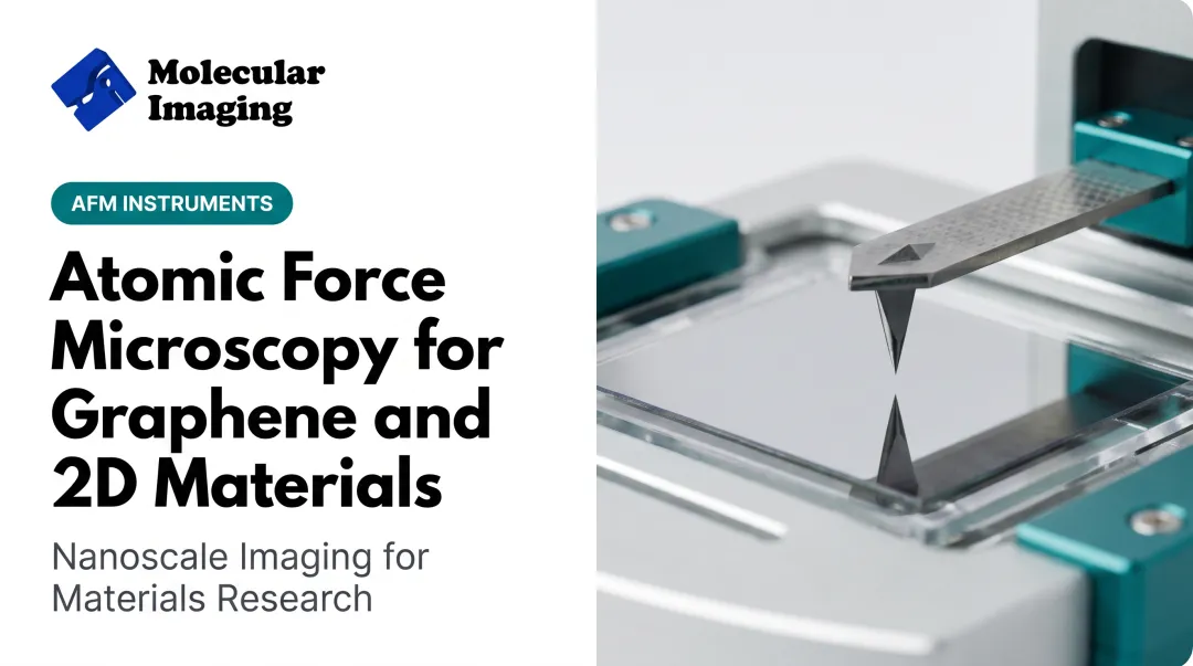
The mechanical side of SCM still relies on standard AFM feedback: a laser reflects off the cantilever onto a position-sensitive photodiode (PSPD), which tracks deflection and keeps the tip at the correct scanning height. The PSPD handles topography; a separate RF/lock-in path handles the capacitance channel. Both need to run in sync. Even with solid feedback, a few sample and bias conditions still dominate what you see in the capacitance channel:

Factors that shift your measured signal:
- Oxide layer thickness
- Depletion layer thickness (tied to dopant concentration)
- Applied AC/DC voltage and frequency
Key Applications of SCM in Research and Industry
SCM’s primary role is dopant and carrier mapping. Related electrical and materials applications build on that same local capacitance signal.
Primary Use: Dopant and Defect Mapping
- Dopant profiling: converts local capacitance modulation into 2D dopant-concentration maps, per NIST’s description of SCM for semiconductor characterization
- Charge carrier concentration mapping across p-n junctions and unipolar samples
- Defect and interface-trap detection: dV/dC mapping on HfSiO/Si structures showed annealing reduced interface-trap variability that averaged measurements miss
Secondary Applications
Beyond dopant maps, analytical models support local dielectric property measurement, including thin-film permittivity from nanoscale capacitance data. In failure analysis, an IEEE case study combined plane-view SCM with nanoprobing and TCAD modeling to diagnose faults in 65 nm and 45 nm MOS process nodes.
Specialized: Cryogenic and High-Field Imaging
Dynamic SCM (DSCM) extends the technique into quantum condensed-matter research. One study imaged compressible and incompressible strips in a GaAs/AlGaAs two-dimensional electron gas at 2.1 K, under perpendicular magnetic fields up to 12 T. That work needs specialized hardware, not a standard room-temperature SCM setup.
Most labs, though, use conventional SCM in semiconductor and materials workflows:
Industries and Research Fields Using SCM
- Semiconductor R&D labs performing dopant and process-node diagnostics
- University surface-science and condensed-matter departments
- Materials science groups studying thin dielectrics and interfaces
- Molecular electronics groups probing nanoscale charge transport (less published SCM evidence than in dopant profiling)

Choosing the Right AFM System for SCM
SCM isn't a bolt-on feature. It demands specific hardware working in concert with your AFM's mechanical feedback loop.
What to look for:
- Modular platform architecture — a system that accepts a capacitance sensor module alongside standard imaging heads, rather than requiring a dedicated instrument
- Multi-mode flexibility — the ability to run AFM, STM, and electrical modes on one platform without swapping instruments between experiments
- Compatible conductive probes — metal-coated tips (Pt/Ir or Co/Cr) that survive contact-mode scanning without degrading
- Calibration and modeling support — reference standards and documentation that account for oxide thickness, depletion physics, and contact regime
- Long-term service access — capacitance electronics and probes wear out, so a service partner who knows the platform matters across a multi-year research program
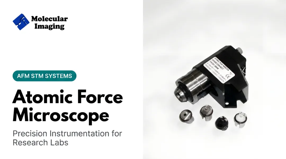
Molecular Imaging's modular AFM/STM systems use interchangeable nose-cone designs so labs can switch between imaging techniques on one platform instead of maintaining separate instruments. The company also provides technical documentation, including modeling guides on SCM dC/dV measurements and interface effects, to help labs interpret their data correctly.

For labs already running legacy Agilent or Molecular Imaging systems, ZoomAFM repair and maintenance support covers diagnostics, calibration, and component replacement. That support keeps capacitance-sensing electronics reliable over multi-year research programs.
If you're configuring a new setup or troubleshooting an existing one, Molecular Imaging's technical support team (1-888-644-0389) can walk through platform-specific questions.
Frequently Asked Questions
What is scanning capacitance microscopy used for?
SCM maps dopant concentration, charge carrier distribution, and defects in semiconductor and MOS device samples. It's also used for local dielectric property measurement and, in specialized setups, quantum electronic structure imaging.
How does scanning capacitance microscopy work?
A metal-coated AFM tip and the sample form a capacitor separated by an oxide dielectric. An applied AC/DC voltage modulates the depletion layer, and a lock-in amplifier detects the resulting dC/dV signal as the tip scans.
What is the difference between SCM and standard AFM?
Standard AFM measures only surface topography through mechanical tip-sample interaction. SCM adds a capacitance-sensing circuit and a metal-coated tip, revealing electrical properties like carrier concentration alongside the topography map.
What materials can be analyzed using SCM?
SCM works best on semiconductors, oxide layers, and MOS structures where the tip-sample junction behaves as a capacitor. It's also used on oxide-free samples, though the Schottky-contact behavior there complicates interpretation.
What resolution can scanning capacitance microscopy achieve?
Published research demonstrates sub-10nm lateral resolution under specific probe and sample conditions, tied to tip geometry and dopant concentration. It's a documented benchmark, not a guaranteed spec across every configuration.
Can SCM be performed on any AFM system?
No. SCM requires a dedicated capacitance sensor module, compatible metal-coated probes, and a platform that can run both mechanical and electrical channels together — not every standard AFM supports this.